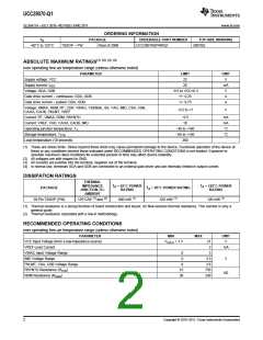
UCC28070-Q1
www.ti.com
SLUSA71A –JULY 2010–REVISED JUNE 2011
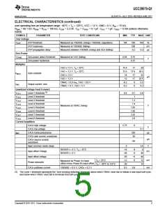
ELECTRICAL CHARACTERISTICS (continued)
over operating free-air temperature range −40°C < TA < 125°C, VCC = 12 V, GND = 0 V, RRT = 75 kΩ,
RDMX = 68.1 kΩ, RRDM = RSYN = 100 kΩ, CCDR = 2.2 nF, CSS = CVREF = 0.1 µF, CVCC = 1 µF, IVREF = 0 mA (unless otherwise
noted)
SYMBOL
PARAMETER
TEST CONDITIONS
MIN
TYP
MAX UNIT
Over Voltage
VOVP
OVP threshold
OVP hysteresis
Measured as VSENSE (rising) / VSENSE (regulation)
Measured at VSENSE (falling)
104
106
100
0.2
108
0.3
%
mV
μs
OVP propagation delay
Measured between VSENSE (rising) and GDx (falling)
Zero-Power
VZPWR
Zero-power detect threshold
Zero-power hysteresis
Measured at VAO (falling)
0.65
0.75
0.15
V
Multiplier
VAO ≥ 1.5 V, TA = 25°C
VAO = 1.2 V, TA = 25°C
VAO ≥ 1.5 V
15.4
13.5
14
17
17.0
17
17
0
20
20.5
22
kMULT
Gain constant
μA
VAO = 1.2 V
12
22.5
0.2
VINAC = 0.9 VPK, VAO = 0.8 V
VINAC = 0 V, VAO = 5 V
-0.2
-0.2
IIMO
Output current: zero
0
0.2
Quantized Voltage Feed Forward
(3)
VLVL1
VLVL2
VLVL3
VLVL4
VLVL5
VLVL6
VLVL7
VLVL8
Level 1 threshold
Level 2 threshold
Level 3 threshold
Level 4 threshold
Level 5 threshold
Level 6 threshold
Level 7 threshold
Level 8 threshold
0.6
0.7
1
0.8
1.2
1.4
Measured at VINAC (rising)
V
1.65
1.95
2.25
2.6
Current Amplifiers
CAOx high voltage
5.75
6
V
CAOx low voltage
0.1
gMC
CAOx transconductance
CAOx sink current, overdriven
100
50
μs
μA
CAOx source current,
overdriven
−50
Input common mode range
Input offset Voltage
Input offset voltage
0
-16
-50
-50
-12
-20
0.5
3.6
0
V
RSYNTH = 6 V, TA = 25°C
-8
-8
−8
0
mV
RSYNTH = 6 V
40
40
TA = 25°C
12 mV
14
Measured as Phase A's input
offset minus Phase B's input offset
Phase mismatch
TA = -40°C to 125°C
CAOx pulldown current
VSENSE = 0.5 V, CAOx = 0.2 V
0.9
mA
(3) The Level 1 threshold represents the "zero-crossing detection" threshold above which VINAC must rise to initiate a new input half-cycle,
and below which VINAC must fall to terminate that half-cycle.
Copyright © 2010–2011, Texas Instruments Incorporated
5

 TI [ TEXAS INSTRUMENTS ]