UCC28070-Q1
SLUSA71A –JULY 2010–REVISED JUNE 2011
www.ti.com
Linear Multiplier
The multiplier of the UCC28070 generates a reference current which represents the desired wave shape and
proportional amplitude of the ac input current. This current is converted to a reference voltage signal by the RIMO
resistor, which is scaled in value to match the voltage of the current-sense signals. The instantaneous multiplier
current is dependent upon the rectified, scaled input voltage VVINAC and the voltage-error amplifier output VVAO
.
The VVINAC signal conveys three pieces of information to the multiplier:
1. The overall wave-shape of the input voltage (typically sinusoidal),
2. The instantaneous input voltage magnitude at any point in the line cycle,
3. The rms level of the input voltage.
The VVAO signal represents the total output power of the PFC pre-regulator.
A major innovation in the UCC28070 multiplier architecture is the internal quantized VRMS feed-forward (QVFF
)
circuitry, which eliminates the requirement for external filtering of the VINAC signal and the subsequent slow
response to transient line variations. A unique circuit algorithm detects the transition of the peak of VVINAC
through seven thresholds and generates an equivalent VFF level centered within the eight QVFF ranges. The
boundaries of the ranges expand with increasing VIN to maintain an approximately equal-percentage delta
between levels. These eight QVFF levels are spaced to accommodate the full "universal" line range of 85 V-265
VRMS
.
A great benefit of the QVFF architecture is that the fixed kVFF factors eliminate any contribution to distortion of the
multiplier output, unlike an externally-filtered VINAC signal which unavoidably contains 2nd-harmonic distortion
components. Furthermore, the QVFF algorithm allows for rapid response to both increasing and decreasing
changes in input rms voltage so that disturbances transmitted to the PFC output are minimized. 5% hysteresis in
the level thresholds help avoid "chattering" between QVFF levels for VVINAC voltage peaks near a particular
threshold or containing mild ringing or distortion. The QVFF architecture requires that the input voltage be largely
sinusoidal, and relies on detecting zero-crossings to adjust QVFF downward on decreasing input voltage.
Zero-crossings are defined as VVINAC falling below 0.7 V for at least 50 μs typically.
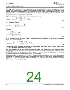
Table 1 reflects the relationship between the various VINAC peak voltages and the corresponding kVFF terms for
the multiplier equation.
Table 1. VINAC Peak Voltages
(1)
LEVEL
VVINAC PEAK VOLTAGE
2.60 V ≤ VVINAC(pk)
kVFF (V2)
3.857
2.922
2.199
1.604
1.156
0.839
0.600
0.398
VIN PEAK VOLTAGE
> 345 V
8
7
6
5
4
3
2
1
2.25 V ≤ VVINAC(pk) < 2.60 V
1.95 V ≤ VVINAC(pk) < 2.25 V
1.65 V ≤ VVINAC(pk) < 1.95 V
1.40 V ≤ VVINAC(pk) < 1.65 V
1.20 V ≤ VVINAC(pk) < 1.40 V
1.00 V ≤ VVINAC(pk) < 1.20 V
300 V to 345 V
260 V to 300 V
220 V to 260 V
187 V to 220 V
160 V to 187 V
133 V to 160 V
< 133 V
VVINAC(pk) ≤ 1.00 V
(1) The VIN peak voltage boundary values listed above are calculated based on a 400-V PFC output voltage and the use of a matched
resistor-divider network (kR = 3 V/400 V = 0.0075) on VINAC and VSENSE (as required for current synthesis). When VOUT is designed
to be higher or lower than 400 V, kR = 3 V/VOUT, and the VIN peak voltage boundary values for each QVFF level adjust to VVINAC(pk)/kR.
22
Copyright © 2010–2011, Texas Instruments Incorporated

 TI [ TEXAS INSTRUMENTS ]