UCC21759-Q1
SLUSEB4A – AUGUST 2020 – REVISED DECEMBER 2020
www.ti.com
hysteresis and UVLO deglitch filter, the internal UVLO protection block will ignore small noises during the normal
switching transients.
The timing diagrams of the UVLO feature of VCC and VDD are shown in Figure 7-8, and Figure 7-9. The RDY
pin on the input side is used to indicate the power good condition. The RDY pin is open drain. During UVLO
condition, the RDY pin is held in low status and connected to GND. Normally the pin is pulled up externally to
VCC to indicate the power good. The AIN-APWM function stops working during the UVLO status. The APWM
pin on the input side will be held LOW.
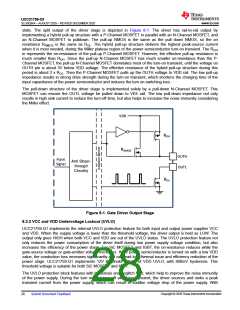
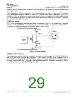
8.3.4 Active Pulldown
UCC21759-Q1 implements an active pulldown feature to ensure the OUTH/OUTL pin clamping to VEE when the
VDD is open. The OUTH/OUTL pin is in high-impedance status when VDD is open, the active pulldown feature
can prevent the output be false turned on before the device is back to control.
VDD
OUTL
Ra
Control
Circuit
VEE
COM
Figure 8-2. Active Pulldown
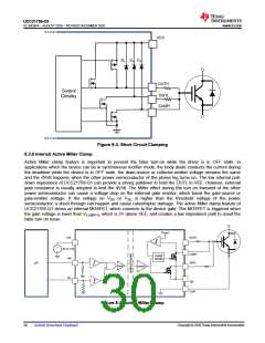
8.3.5 Short Circuit Clamping
During short circuit condition, the Miller capacitance can cause a current sinking to the OUTH/OUTL/CLMPI pin
due to the high dV/dt and boost the OUTH/OUTL/CLMPI voltage. The short circuit clamping feature of
UCC21759-Q1 can clamp the OUTH/OUTL/CLMPI pin voltage to be slightly higher than VDD, which can protect
the power semiconductors from a gate-source and gate-emitter overvoltage breakdown. This feature is realized
by an internal diode from the OUTH/OUTL/CLMPI to VDD.
Copyright © 2020 Texas Instruments Incorporated
Submit Document Feedback
29

 TI [ TEXAS INSTRUMENTS ]