UCC21759-Q1
SLUSEB4A – AUGUST 2020 – REVISED DECEMBER 2020
www.ti.com
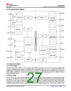
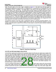
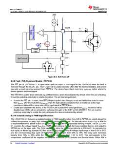
state. The split output of the driver stage is depicted in Figure 8-1. The driver has rail-to-rail output by
implementing a hybrid pull-up structure with a P-Channel MOSFET in parallel with an N-Channel MOSFET, and
an N-Channel MOSFET to pulldown. The pull-up NMOS is the same as the pull down NMOS, so the on
resistance RNMOS is the same as ROL. The hybrid pull-up structure delivers the highest peak-source current
when it is most needed, during the Miller plateau region of the power semiconductor turn-on transient. The ROH
in represents the on-resistance of the pull-up P-Channel MOSFET. However, the effective pull-up resistance is
much smaller than ROH. Since the pull-up N-Channel MOSFET has much smaller on-resistance than the P-
Channel MOSFET, the pull-up N-Channel MOSFET dominates most of the turn-on transient, until the voltage on
OUTH pin is about 3V below VDD voltage. The effective resistance of the hybrid pull-up structure during this
period is about 2 x ROL. Then the P-Channel MOSFET pulls up the OUTH voltage to VDD rail. The low pull-up
impedance results in strong drive strength during the turn-on transient, which shortens the charging time of the
input capacitance of the power semiconductor and reduces the turn on switching loss.
The pull-down structure of the driver stage is implemented solely by a pull-down N-Channel MOSFET. This
MOSFET can ensure the OUTL voltage be pulled down to VEE rail. The low pull-down impedance not only
results in high sink current to reduce the turn-off time, but also helps to increase the noise immunity considering
the Miller effect.
VDD
ROH
RNMOS
OUTH
Input
Signal
Anti Shoot-
through
Circuitry
OUTL
ROL
Figure 8-1. Gate Driver Output Stage
8.3.3 VCC and VDD Undervoltage Lockout (UVLO)
UCC21759-Q1 implements the internal UVLO protection feature for both input and output power supplies VCC
and VDD. When the supply voltage is lower than the threshold voltage, the driver output is held as LOW. The
output only goes HIGH when both VCC and VDD are out of the UVLO status. The UVLO protection feature not
only reduces the power consumption of the driver itself during low power supply voltage condition, but also
increases the efficiency of the power stage. For SiC MOSFET and IGBT, the on-resistance reduces while the
gate-source voltage or gate-emitter voltage increases. If the power semiconductor is turned on with a low VDD
value, the conduction loss increases significantly and can lead to a thermal issue and efficiency reduction of the
power stage. UCC21759-Q1 implements 12V threshold voltage of VDD UVLO, with 800mV hysteresis. This
threshold voltage is suitable for both SiC MOSFET and IGBT.
The UVLO protection block features with hysteresis and deglitch filter, which help to improve the noise immunity
of the power supply. During the turn on and turn off switching transient, the driver sources and sinks a peak
transient current from the power supply, which can result in sudden voltage drop of the power supply. With
Copyright © 2020 Texas Instruments Incorporated
28
Submit Document Feedback

 TI [ TEXAS INSTRUMENTS ]