UCC21759-Q1
SLUSEB4A – AUGUST 2020 – REVISED DECEMBER 2020
www.ti.com
VDD
DESAT
R
DHV
+
CBLK
+
VDESAT
œ
Control
Logic
COM
OUTL
Soft Turn-off
VEE
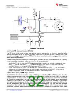
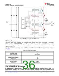
Figure 8-6. Soft Turn-off
8.3.9 Fault ( FLT, Reset and Enable ( RST/EN)
The FLT pin of UCC21759-Q1 is open drain and can report a fault signal to the DSP/MCU when the fault is
detected through the DESAT pin. The FLT pin will be pulled down to GND after the fault is detected, and is held
low until a reset signal is received from RST/EN. The device has a fault mute time tFLTMUTE, within which the
device ignores any reset signal.
The RST/EN is pulled down internally by a 50kΩ resistor, and is thus disabled by default when this pin is floating.
It must be pulled up externally to enable the driver. The pin has two purposes:
•
To reset the FLT pin. To reset, then RST/EN pin is pulled low; if the pin is set and held in low state for more
than tRSTFIL after the mute time tFLTMUTE, then the fault signal is reset and FLT is reset back to the high
impedance status at the rising edge of the input signal at RST/EN pin.
•
Enable and shutdown the device. If the RST/EN pin is pulled low for longer than tRSTFIL, the driver will be
disabled and OUTL will be activated to pull down the gate of the IGBT or SiC MOSFET. The pin must be
pulled up externally to enable the part, otherwise the device is disabled by default.
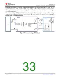
8.3.10 Isolated Analog to PWM Signal Function
The UCC21759-Q1 features an isolated analog to PWM signal function from AIN to APWM pin, which allows the
isolated temperature sensing, high voltage dc bus voltage sensing, etc. An internal current source IAIN in AIN pin
is implemented in the device to bias an external thermal diode or temperature sensing resistor. The UCC21759-
Q1 encodes the voltage signal VAIN to a PWM signal, passing through the basic isolation barrier, and output to
APWM pin on the input side. The PWM signal can either be transferred directly to DSP/MCU to calculate the
duty cycle, or filtered by a simple RC filter as an analog signal. The AIN voltage input range is from 0.6V to 4.5V,
and the corresponding duty cycle of the APWM output ranges from 88% to 10%. The duty cycle increases
linearly from 10% to 88% while the AIN voltage decreases from 4.5V to 0.6V. This corresponds to the
temperature coefficient of the negative temperature coefficient (NTC) resistor and thermal diode. When AIN is
Copyright © 2020 Texas Instruments Incorporated
32
Submit Document Feedback

 TI [ TEXAS INSTRUMENTS ]