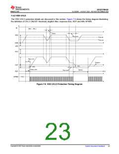
UCC21759-Q1
SLUSEB4A – AUGUST 2020 – REVISED DECEMBER 2020
www.ti.com
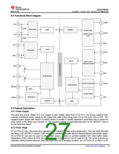
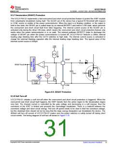
8.2 Functional Block Diagram
CLMPI
OUTH
7
4
6
10
11
15
9
IN+
INt
55kQ
55kQ
PWM Inputs
MOD
DEMOD
Output Stage
t
ON/OFF Control
STO
VCC
OUTL
VDD
VCC
UVLO
VCC Supply
5
GND
RDY
UVLO
LDO[s for VEE,
COM and channel
3
8
COM
VEE
12
13
14
16
Fault Decode
FLT
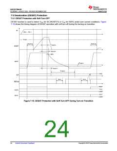
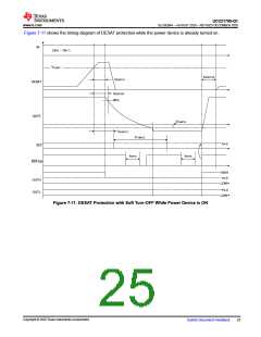
DESAT Protection
Analog 2 PWM
2
DESAT
Fault Encode
RST/EN
50kQ
PWM Driver
AIN
1
APWM
DEMOD
MOD
8.3 Feature Description
8.3.1 Power Supply
The input side power supply VCC can support a wide voltage range from 3V to 5.5V. The device supports both
unipolar and bipolar power supply on the output side, with a wide range from 13V to 33V from VDD to VEE. The
negative power supply with respect to switch source or emitter is usually adopted to avoid false turn on when the
other switch in the phase leg is turned on. The negative voltage is especially important for SiC MOSFET due to
its fast switching speed.
8.3.2 Driver Stage
UCC21759-Q1 has ±10A peak drive strength and is suitable for high power applications. The high drive strength
can drive a SiC MOSFET module, IGBT module or paralleled discrete devices directly without extra buffer stage.
UCC21759-Q1 can also be used to drive higher power modules or parallel modules with extra buffer stage.
Regardless of the values of VDD, the peak sink and source current can be kept at 10A. The driver features an
important safety function wherein, when the input pins are in floating condition, the OUTH/OUTL is held in LOW
Copyright © 2020 Texas Instruments Incorporated
Submit Document Feedback
27

 TI [ TEXAS INSTRUMENTS ]