PDF
最近搜索
热门搜索
发布采购

| 型号: | UCC21759QDWRQ1 |
| PDF下载: | 下载PDF文件 查看货源 |
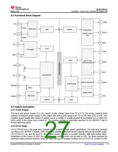
| 内容描述: | [适用于 IGBT/SiC MOSFET 且具有 DESAT 和内部钳位的汽车类 3.0kVrms、±10A 单通道隔离式栅极驱动器 | DW | 16 | -40 to 150] |
| 分类和应用: | 栅极驱动双极性晶体管驱动器 |
| 文件页数/大小: | 57 页 / 2481 K |
| 品牌: |  TI [ TEXAS INSTRUMENTS ] TI [ TEXAS INSTRUMENTS ] |
专业IC领域供求交易平台:提供全面的IC Datasheet资料和资讯,Datasheet 1000万数据,IC品牌1000多家。