UC2625-EP
www.ti.com .................................................................................................................................................................................................. SLUS802–MARCH 2008
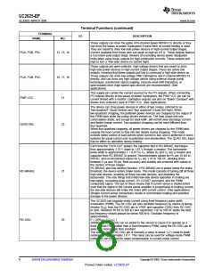
Terminal Functions (continued)
TERMINAL
I/O
DESCRIPTION
NAME
NO.
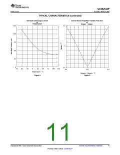
Any time that VCC drops below threshold or the sensed current exceeds the
over-current threshold, the soft-start latch is set. When set, it turns on a transistor
that pulls down on SSTART. Normally, a capacitor is connected to this pin, and the
transistor will completely discharge the capacitor. A comparator senses when the
NPN transistor has completely discharged the capacitor, and allows the soft-start
latch to clear when the fault is removed. When the fault is removed, the soft-start
capacitor charges from the on-chip current source.
SSTART clamps the output of the error amplifier, not allowing the error amplifier
output voltage to exceed SSTART regardless of input. The ramp on RC-OSC can
be applied to PWM In and compared to E/A OUT. With SSTART discharged below
0.2 V and the ramp minimum being approximately 1.0 V, the PWM comparator
keeps the PWM latch cleared and the outputs off. As SSTART rises, the PWM
comparator begins to duty-cycle modulate the PWM latch until the error amplifier
inputs overcome the clamp. This provides for a safe and orderly motor start-up
from an off or fault condition. A 51-kΩ resister is added between VREF and
SSTART to ensure switching.
SSTART
24
Any change in the H1, H2, or H3 inputs loads data from these inputs into the
position sensor latches. At the same time data is loaded, a fixed-width 5-V pulse is
triggered on TACH-OUT. The average value of the voltage on TACH-OUT is
directly proportional to speed, so this output can be used as a true tachometer for
speed feedback with an external filter or averaging circuit which usually consists of
a resistor and capacitor.
TACH-OUT
20
Whenever TACH-OUT is high, the position latches are inhibited, such that during
the noisiest part of the commutation cycle, additional commutations are not
possible. Although this effectively sets a maximum rotational speed, the maximum
speed can be set above the highest expected speed, preventing false commutation
and chatter.
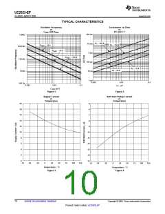
This device operates with supplies between 10 V and 18 V. Under-voltage lockout
keeps all outputs off below 7.5 V, insuring that the output transistors never turn on
until full drive capability is available. Bypass VCC to ground with an 0.1-µF ceramic
capacitor. Using a 10-µF electrolytic bypass capacitor as well can be beneficial in
applications with high supply impedance.
VCC
19
2
This pin provides regulated 5 V for driving Hall-effect devices and speed control
circuitry. VREF reaches 5 V before VCC enables, ensuring that Hall-effect devices
powered from VREF becomes active before the UC3625 drives any output. For
proper performance VREF should be bypassed with at least a 0.1-µF capacitor to
ground.
VREF
Copyright © 2008, Texas Instruments Incorporated
Submit Documentation Feedback
9
Product Folder Link(s) :UC2625-EP

 TI [ TEXAS INSTRUMENTS ]