UC2625-EP
SLUS802–MARCH 2008 .................................................................................................................................................................................................. www.ti.com
APPLICATION INFORMATION
Cross Conduction Prevention
The UC2625 inserts delays to prevent cross conduction due to overlapping drive signals. However, some thought
must always be given to cross conduction in output stage design because no amount of dead time can prevent
fast slewing signals from coupling drive to a power device through a parasitic capacitance.
The UC2625 contains input latches that serve as noise blanking filters. These latches remain transparent through
any phase of a motor rotation and latch immediately after an input transition is detected. They remain latched for
two cycles of the PWM oscillator. At a PWM oscillator speed of 20 kHz, this corresponds to 50 µs to 100 µs of
blank time which limits maximum rotational speed to 100 kRPM for a motor with six transitions per rotation or 50
kRPM for a motor with 12 transitions per rotation.
This prevents noise generated in the first 50 µs of a transition from propagating to the output transistors and
causing cross-conduction or chatter.
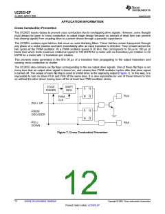
The UC2625 also contains six flip flops corresponding to the six output drive signals. One of these flip flops is set
every time that an output drive signal is turned on, and cleared two PWM oscillator cycles after that drive signal
is turned off. The output of each flip flop is used to inhibit drive to the opposing output (Figure 7). In this way, it is
impossible to turn on driver PUA and PDA at the same time. It is also impossible for one of these drivers to turn
on without the other driver having been off for at least two PWM oscillator clocks.
EDGE
FINDER
SHIFT
REG
S
R
Q
Q
PUA
PWM
CLK
PULL UP
S
R
Q
Q
FROM
DECODER
PULL
PDA
DOWN
Figure 7. Cross Conduction Prevention
12
Submit Documentation Feedback
Copyright © 2008, Texas Instruments Incorporated
Product Folder Link(s) :UC2625-EP

 TI [ TEXAS INSTRUMENTS ]