TUSB1310A
SLLSE32D–NOVEMBER 2010–REVISED MAY 2011
www.ti.com
1.3 Introduction
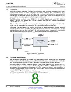
The TUSB1310A is a single port, 5.0-Gbps USB 3.0 physical layer transceiver operating off of a single
reference clock provided by either a crystal or an external reference clock. The reference clock
frequencies are selectable from 20, 25, 30, and 40 MHz. The TUSB1310A provides the clock to the USB
controller. The use of a single reference clock allows the TUSB1310A to provide a cost effective USB 3.0
solution with few external components and a low implementation cost.
The USB controller interfaces to the TUSB1310A via a PIPE (SuperSpeed) and a ULPI (USB2.0)
interface. The 16-bit PIPE operates off of a 250-MHz interface clock. The ULPI supports 8-bit operations
with a 60-MHz interface clock.
USB 3.0 reduces active and idle power consumption with improved power management features. The
TUSB1310A low power states are controlled by the USB controller via the PIPE interface.
SuperSpeed USB uses existing USB software infrastructure by keeping the existing software interfaces
and software drivers intact. In addition, SuperSpeed USB retains backward compatibility with USB 2.0
based products by using the same form-factor Type-A connector and cables. Existing USB 2.0 devices will
work with new USB 3.0 hosts and new USB 3.0 devices with work with legacy USB 2.0 hosts.
Crystal
PIPE
(16 bit 250 MHz)
SSTX P/N
SSRX P/N
5.0 Gbps
TUSB1310A
MCU/CPU
ULPI
DP/DM
(8 bit 60 MHz)
CLKOUT
Figure 1-1. Typical Application
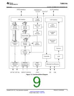
1.4 Functional Block Diagram
The USB physical layer handles the low level USB protocol and signaling. This includes data serialization
and deserialization, 8b/10b encoding, analog buffers, elastic buffers and receiver detection. It shifts the
clock domain of the data from the USB rate to one that is compatible with the link layer controller.
The SuperSpeed USB contains SSTXP/SSTXN and SSRXP/SSRXP differential pairs and uses the PIPE
to communicate with the link layer controller. The Non-SuperSpeed USB has a DP/DM differential pair and
communicates with the link layer controller via the ULPI. The TUSB1310A reference clock is connected to
an internal crystal oscillator, spread spectrum clock and PLL which provides clocks to all functional blocks
and to the CLKOUT pin for the link layer controller.
A JTAG interface is used for IEEE1149.1 and IEEE1149.6 boundary scan.
8
PRODUCT OVERVIEW
Copyright © 2010–2011, Texas Instruments Incorporated
Submit Documentation Feedback
Product Folder Link(s): TUSB1310A

 TI [ TEXAS INSTRUMENTS ]