TPS929160-Q1
ZHCSNG0 – APRIL 2023
www.ti.com.cn
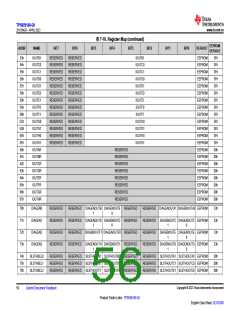
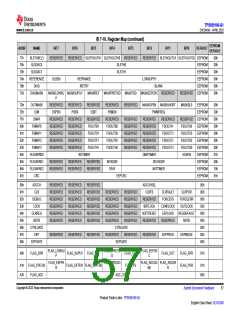
表 7-19. BRT Registers (continued)
Offset
30h
31h
32h
33h
34h
35h
36h
37h
40h
41h
42h
43h
44h
Acronym
Register Name
Section
Go
PWMLR0
PWMLR1
PWMLR2
PWMLR3
PWMLR4
PWMLR5
PWMLR6
PWMLR7
OUTEN0
OUTEN1
OUTEN2
OUTEN3
PWMSHARE
Reserved Register
Reserved Register
Go
Reserved Register
Go
Reserved Register
Go
Reserved Register
Go
Reserved Register
Go
Reserved Register
Go
Reserved Register
Go
OUTAn, OUTBn Enable Setting
OUTCn, OUTDn Enable Setting
OUTEn, OUTFn Enable Setting
OUTGn, OUTHn Enable Setting
Go
Go
Go
Go
PWM Duty-cycle Sharing for All Enabled Output
Go
Complex bit access types are encoded to fit into small table cells. 表 7-20 shows the codes that are used for
access types in this section.
表 7-20. BRT Access Type Codes
Access Type
Read Type
R
Code
Description
R
Read
Write Type
W
W
Write
Reset or Default Value
-n
Value after reset or the default
value
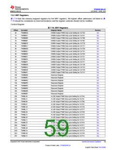
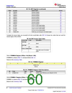
7.6.1.1 PWMMA0 Register (Offset = 0h) [Reset = 00h]
PWMMA0 is shown in 图 7-21 and described in 表 7-21.
Return to the Summary Table.
图 7-21. PWMMA0 Register
7
6
5
4
3
2
1
0
PWMOUTA0
R/W-0h
表 7-21. PWMMA0 Register Field Descriptions
Bit
7-0
Field
PWMOUTA0
Type
Reset
Description
R/W
0h
8-MSB output PWM duty-cycle setting for OUTA0
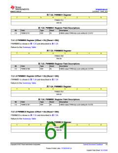
7.6.1.2 PWMMA1 Register (Offset = 1h) [Reset = 00h]
PWMMA1 is shown in 图 7-22 and described in 表 7-22.
Return to the Summary Table.
Copyright © 2023 Texas Instruments Incorporated
English Data Sheet: SLVSG60
60
Submit Document Feedback
Product Folder Links: TPS929160-Q1

 TI [ TEXAS INSTRUMENTS ]