TPS929160-Q1
ZHCSNG0 – APRIL 2023
www.ti.com.cn
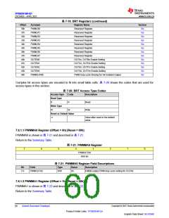
7.6.1 BRT Registers
表 7-19 lists the memory-mapped registers for the BRT registers. All register offset addresses not listed in 表
7-19 should be considered as reserved locations and the register contents should not be modified.
Control Register
表 7-19. BRT Registers
Offset
0h
Acronym
PWMMA0
PWMMA1
PWMMB0
PWMMB1
PWMMC0
PWMMC1
PWMMD0
PWMMD1
PWMME0
PWMME1
PWMMF0
PWMMF1
PWMMG0
PWMMG1
PWMMH0
PWMMH1
PWMMR0
PWMMR1
PWMMR2
PWMMR3
PWMMR4
PWMMR5
PWMMR6
PWMMR7
PWMLA0
PWMLA1
PWMLB0
PWMLB1
PWMLC0
PWMLC1
PWMLD0
PWMLD1
PWMLE0
PWMLE1
PWMLF0
PWMLF1
PWMLG0
PWMLG1
PWMLH0
PWMLH1
Register Name
Section
Go
Go
Go
Go
Go
Go
Go
Go
Go
Go
Go
Go
Go
Go
Go
Go
Go
Go
Go
Go
Go
Go
Go
Go
Go
Go
Go
Go
Go
Go
Go
Go
Go
Go
Go
Go
Go
Go
Go
Go
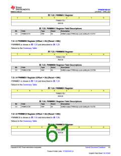
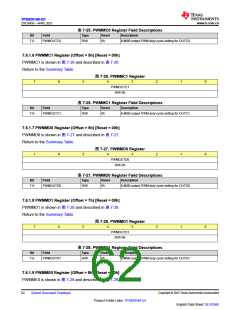
8-MSB Output PWM Duty-cycle Setting for OUTA0
8-MSB Output PWM Duty-cycle Setting for OUTA1
8-MSB Output PWM Duty-cycle Setting for OUTB0
8-MSB Output PWM Duty-cycle Setting for OUTB1
8-MSB Output PWM Duty-cycle Setting for OUTC0
8-MSB Output PWM Duty-cycle Setting for OUTC1
8-MSB Output PWM Duty-cycle Setting for OUTD0
8-MSB Output PWM Duty-cycle Setting for OUTD1
8-MSB Output PWM Duty-cycle Setting for OUTE0
8-MSB Output PWM Duty-cycle Setting for OUTE1
8-MSB Output PWM Duty-cycle Setting for OUTF0
8-MSB Output PWM Duty-cycle Setting for OUTF1
8-MSB Output PWM Duty-cycle Setting for OUTG0
8-MSB Output PWM Duty-cycle Setting for OUTG1
8-MSB Output PWM Duty-cycle Setting for OUTH0
8-MSB Output PWM Duty-cycle Setting for OUTH1
Reserved Register
1h
2h
3h
4h
5h
6h
7h
8h
9h
Ah
Bh
Ch
Dh
Eh
Fh
10h
11h
12h
13h
14h
15h
16h
17h
20h
21h
22h
23h
24h
25h
26h
27h
28h
29h
2Ah
2Bh
2Ch
2Dh
2Eh
2Fh
Reserved Register
Reserved Register
Reserved Register
Reserved Register
Reserved Register
Reserved Register
Reserved Register
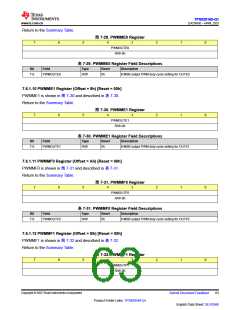
4-LSB Output PWM Duty-cycle Setting for OUTA0
4-LSB Output PWM Duty-cycle Setting for OUTA1
4-LSB Output PWM Duty-cycle Setting for OUTB0
4-LSB Output PWM Duty-cycle Setting for OUTB1
4-LSB Output PWM Duty-cycle Setting for OUTC0
4-LSB Output PWM Duty-cycle Setting for OUTC1
4-LSB Output PWM Duty-cycle Setting for OUTD0
4-LSB Output PWM Duty-cycle Setting for OUTD1
4-LSB Output PWM Duty-cycle Setting for OUTE0
4-LSB Output PWM Duty-cycle Setting for OUTE1
4-LSB Output PWM Duty-cycle Setting for OUTF0
4-LSB Output PWM Duty-cycle Setting for OUTF1
4-LSB Output PWM Duty-cycle Setting for OUTG0
4-LSB Output PWM Duty-cycle Setting for OUTG1
4-LSB Output PWM Duty-cycle Setting for OUTH0
4-LSB Output PWM Duty-cycle Setting for OUTH1
Copyright © 2023 Texas Instruments Incorporated
Submit Document Feedback
59
Product Folder Links: TPS929160-Q1
English Data Sheet: SLVSG60

 TI [ TEXAS INSTRUMENTS ]