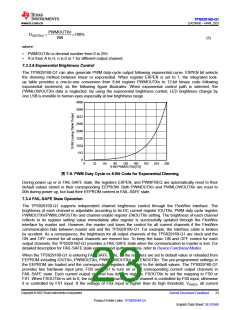
TPS929160-Q1
ZHCSNG0 – APRIL 2023
www.ti.com.cn
7.3.5.2 ADC Auto Scan
In ADC auto scan mode, If the MAXOUT channel is selected by writing 06h to ADCCHSEL, the maximum
voltage of OUTXn is recorded into ADC_OUT register. The maximum channel output voltage is available
after at least nine output PWM cycles are completed. The ADC measures every two outputs as one group
when the group is turned on and move to measure the next group in next PWM dimming cycle until all eight
groups are completed no matter in PWM dimming mode or phase shift PWM dimming mode. The device sets
FLAG_ADCDONE to 1 and stops ADC auto scan after the measurements for all eight groups are done. The
FLAG_ADCDONE is cleared to 0 by reading the ADC_OUT, and ADC auto scan restarts again if the data of
ADCCHSEL is still 06h. FLAG_ADCDONE is also cleared to 0 by writing ADCCHSEL register, and ADC restarts
after FLAG_ADCDONE is cleared. The minimum current pulse for each output must be longer than t(BLANK) + 3 ×
t (CONV) in auto scan mode. The channel is skipped if it is disabled in auto scan mode.
Based on the measured maximum output voltage and supply voltage, the microcontroller is able to regulate
supply voltage from previous power stage to minimize the power consumption on the TPS929160-Q1. Basically,
the microcontroller must program the output voltage of previous power stage to be just higher than the measured
maximum channel output voltage plus the required dropout voltage V(OUT_drop) of the TPS929160-Q1. In this
way, the TPS929160-Q1 takes minimum power consumption, and overall power efficiency optimizes.
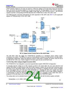
7.3.5.3 ADC Error
The TPS929160-Q1 integrates a digital comparator to measure the PWM dimming period t(DIM_cycle) and t(BLANK)
+ 3 × t(CONV) at real time when ADC is started by writing ADCCHSEL register or reading ADC_OUT register. The
device stops the ADC measurement and sets the FLAG_ADCERR register to 1 if the t(DIM_cycle) time is measured
less than t(BLANK) + 3 × t(CONV) time. The FLAG_ADCERR register is cleared to 0 by writing 1 to the CLRFAULT
register.
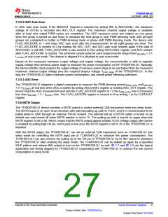
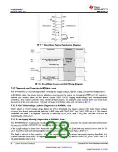
7.3.6 NSTB Output
The TPS929160-Q1 device provides a NSTB output to control external CAN transciever enter into sleep mode.
The NSTB ouput is an open drain structure with internal pulling up path to VLDO, and it is recommended to be
pulled down to GND through an external 100-kΩ resistor. The internal pull up of NSTB output is turned on by
default and only turned off when NSTB register is set to 1h. The pulling up path is turned on again when the
NSTB register is set to 0h. Which means that the NSTB output always exhibits VLDO voltage output after device
is enabled by pulling high EN pin, and it goes to low once the NSTB register is set to 1h or the TPS929160-Q1 is
disabled.
With this NSTB output, the TPS929160-Q1 can set an external CAN transciever such as TCAN1043-Q1 into
sleep mode by controlling the nSTB input pin of TCAN1043-Q1 to minimize the power consumption. The
TCAN1043-Q1 can also remove the pulling up of the EN pin of TPS929160-Q1 by its INH output to shutdown
the TPS929160-Q1 after entering the sleep mode. The TCAN1043-Q1 can be waked up again by a specified
WUP pattern and release INH output to turn on the TPS929160-Q1 as well. 图 7-7 and 图 7-8 are the typical
application and timing diagram for TPS929160-Q1 cooperating with TCAN1043-Q1 to achieve the low current
consumption in sleep mode.
Copyright © 2023 Texas Instruments Incorporated
Submit Document Feedback
27
Product Folder Links: TPS929160-Q1
English Data Sheet: SLVSG60

 TI [ TEXAS INSTRUMENTS ]