TPS929160-Q1
ZHCSNG0 – APRIL 2023
www.ti.com.cn
output channels mapped to FSx input are turned on. When the voltage of FSx input drops below low threshold,
VIL(IO), all current out channels mapped to FSx input are turned off. The flag register FLAG_EXTFSx shows the
FSx input level at real-time. If FSx pin input voltage is logic high, the FLAG_EXTFSx is set to 1. All FSOUTXn
registers load their corresponding EEPROM data when the TPS929160-Q1 enters FAIL-SAFE state.
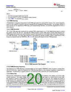
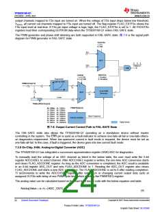
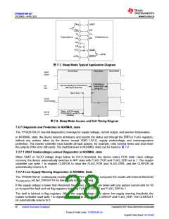
The PWM generator and phase shift dimming are both supported in FAIL-SAFE state. 图 7-6 is the signal path
diagram for PWM generator in FAIL-SAFE state.
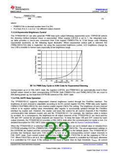
FSOUTXn
1: FS1
0: FS0
FS1
1
MUX
FS0
PWMOUT
0
AND
ENOUTXn
1: Enabled
0: Disabled
EXPEN
1: LUT EN
0: LUT DIS
Exponential
Look-Up Table
PWMOUTXn[7:0]
1
8
8
12
12-bit PWM
Generator
MUX
0
8
12
12
Linear
12
PWMLOWOUTXn[3:0]
PWMFREQ[3:0]
0h: 200Hz 8h: 1000Hz
1h: 250Hz 9h: 1200Hz
2h: 300Hz Ah: 2000Hz
3h: 350Hz Bh: 4000Hz
4h: 400Hz Ch: 5900Hz
5h: 500Hz Dh: 7800Hz
6h: 600Hz Eh: 9600Hz
7h: 800Hz Fh: 20800Hz
Base Frequency
Internal Oscillator
Digital blocks
图 7-6. Output Current Control Path in FAIL-SAFE State
The FAIL-SAFE state also allows the TPS929160-Q1 operating as a standalone device without master
controlling in the system. The ERR pin is used as a fault indicator to achieve one-fails-all-fail or one-fails-others-
on diagnostics requirement. When low quiescent current in fault mode is required, the device must be set as
one-fails-all-fail. In this case, if fault is triggered, the device goes into low current fault mode.
7.3.5 On-Chip, 8-Bit, Analog-to-Digital Converter (ADC)
The TPS929160-Q1 has integrated a successive-approximation-register (SAR) ADC for diagnostics.
To manually read the voltage of an ADC channel as listed in the below table, the user must write the 5-bit
register ADCCHSEL to select channel. After ADCCHSEL register is written, the one-time ADC conversion starts
and clears FLAG_ADCDONE register. As long as the ADC conversion is completed, the ADC result is available
in an 8-bit register ADC_OUT and sets FLAG_ADCDONE to 1. Reading the ADC_OUT register also clears
FLAG_ADCDONE and starts a new ADC conversion. The FLAG_ADCDONE is set to 0 after reading completion.
TI recommends to write the ADCCHSEL register after turning on or changing current output duty cycle at
assigned OUTXn with delay of one PWM cycle time which is set by the PWMFREQ register.
The analog value can be calculated based on the read back binary code with the below equation and table.
AnalogValue = a + k ì ADC_OUT
(
)
(6)
Copyright © 2023 Texas Instruments Incorporated
English Data Sheet: SLVSG60
24
Submit Document Feedback
Product Folder Links: TPS929160-Q1

 TI [ TEXAS INSTRUMENTS ]