TPS929160-Q1
ZHCSNG0 – APRIL 2023
www.ti.com.cn
表 7-3. Phase Shift Dimming Groups
Phase
Phase 0
Groups
Output Channels
OUTA1
Group A
Group B
Group C
Group D
Group E
Group F
Group G
Group H
OUTA0
OUTB0
OUTC0
OUTD0
OUTE0
OUTF0
OUTG0
OUTH0
Phase 1
OUTB1
Phase 2
OUTC1
Phase 3
OUTD1
Phase 4
OUTE1
Phase 5
OUTF1
Phase 6
OUTG1
Phase 7
OUTH1
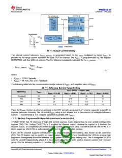
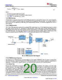
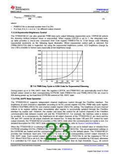
The phase delay interval is 1/8 of PWM dimming cycle time between two neighboring groups. The phase delay
can be calculated with the below equation.
1
T
=
(Delay)
8ìF
(PWM)
(3)
where
F(PWM) is PWM dimming frequency set by PWMFREQ.
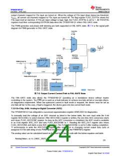
7.3.3.5 Linear Brightness Control
•
When register EXPEN is set to 0, the MSB 8 bits of 12-bit binary input to PWM generator are directly copied
from 8-bit register PWMOUTXn, and the LSB 4 bits are directly copied from 4-bit register PWMLOWOUTXn.
The PWM output duty cycle can be calculated with the following equation. The PWM output duty cycle is
linearly controlled by the register PWMOUTXn and PWMLOWOUTXn, which provides the linear brightness
control to each channel output. When PWMOUTXn is FFh, and PWMLOWOUTXn is Fh, the duty cycle is 100%
exceptionally.
16ìPWMOUTXn + PWMLOWOUTXn
(
)
ì100%
D(OUTXn)
=
4096
(4)
where
•
•
•
PWMOUTXn is decimal number from 0 to 255.
PWMLOWOUTXn is decimal number from 0 to 15.
X is from A to H, n is 0 or 1 for different output channel.
Because the 12-bit PWM duty cycles require 2 bytes of write operation to update the completed data, the output
PWM duty cycle is not changed in between of the two bytes data transmission. TPS929160-Q1 only updates
PWM duty cycle of any output when its high 8-bit PWMOUTXn is written. When very fast brightness change
is needed, for example, fade-in and fade-out effects, simultaneous PWM duty cycle change of all channels is
required. Setting SHAREPWM to 1 enables all channels using the PWM duty cycle setting of channel A0 to save
communication latency. When disabling the SHAREPWM, PWM outputs of all the channels remain unchanged
until the corresponding PWM duty cycle setting registers are modified.
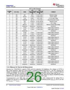
To reduce the data transmission for large quantity of the LED pixel control, 8-bit PWM duty cyle resolution can be
adopted by writing 0 to 12BIT in DIM register. The master only needs to update high 8-bit PWMOUTXn register
to change the brightness of target output channel. The low 4-bit registers PWMLOWOUTXn are ignored. The
PWM duty-cycle calculation is shown in he below equation. When PWMOUTXn is FFh, the duty cycle is 100%
exceptionally.
Copyright © 2023 Texas Instruments Incorporated
English Data Sheet: SLVSG60
22
Submit Document Feedback
Product Folder Links: TPS929160-Q1

 TI [ TEXAS INSTRUMENTS ]