TPS7H5005-SEP, TPS7H5006-SEP, TPS7H5007-SEP, TPS7H5008-SEP
www.ti.com
SLVSGG1 – FEBRUARY 2022
side as 170 V for this application based on maximum input voltage of 36 V. This was to account for any transient
spikes that were seen during operation. Also ensure that the GaN FETs are properly sized based on the primary
current calculations in Section 9.2.2.6.
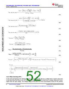
9.2.2.8 Synchronous Rectificier FETs
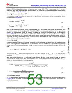
The maximum voltage stress that will be seen by the synchronous rectifier switch on the secondary side can be
calculated using Equation 55.
V
IN_MAX
VSR_STRESS = VOUT
+
NPS
(55)
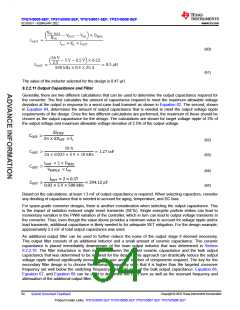
(56)
36 V
VSR_STRESS = 5 V +
= 19.4 V
2.5
Note that the maximum expected voltage is approximately 20 V, but a higher rating should be selected to allow
for transient spikes. For the design, an 80-V rated GaN FET was conservatively chosen for the synchronous
rectifier. The current rating should be sufficient to handle the maximum secondary current as calculated in
Section 9.2.2.6. In order to reduce the current through GaN FET during the soft-start period, when the controller
SRA and SRB signals are off, a Schottky diode can be used in parallel with the synchronous rectifier GaN FETs.
This diode would also mitigate the reverse conduction losses attributed to the GaN FET during the dead time
and boost the overall efficiency of the system.
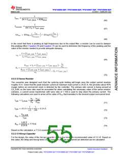
9.2.2.9 RCD Clamp
A resistor-capacitor-diode clamp circuit can be used to limit the voltage at the switch node. The equations below
can be used to determine initial values for the resistor and capacitor, but the circuit will need to be optimized
through testing. First, calculate the clamp voltage by determining how much overshoot is allowable at the switch
node.
(57)
The parameter KCLAMP defines the target overshoot value. For example, set KCLAMP to 1.5 for 50% allowable
overshoot.
Next, the leakage inductance LL and peak primary current IPRI_MAX of the transformer can be used to
approximate the clamp resistor. The clamp capacitor value can be determined thereafter. Note that ΔVCLAMP
defines the allowable ripple for the clamp capacitor.
(58)
VCLAMP
CCLAMP
=
VCLAMP × VCLA MP × RCLAMP × fsw
(59)
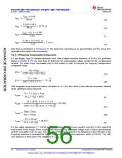
9.2.2.10 Output Inductor
For the output inductor, a ripple current of 40% was targeted for the design. Based on the selected ripple current,
Equation 60 can be used to determine the output inductor value. KL is the current ripple factor, which will be set
to 0.4 in this instance.
Copyright © 2022 Texas Instruments Incorporated
Submit Document Feedback
53
Product Folder Links: TPS7H5005-SEP TPS7H5006-SEP TPS7H5007-SEP TPS7H5008-SEP

 TI [ TEXAS INSTRUMENTS ]