TPS7H5005-SEP, TPS7H5006-SEP, TPS7H5007-SEP, TPS7H5008-SEP
SLVSGG1 – FEBRUARY 2022
www.ti.com
(60)
(61)
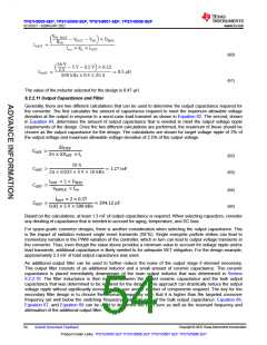
The value of the inductor selected for the design is 0.47 μH.
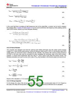
9.2.2.11 Output Capacitance and Filter
Generally, there are two different calculations that can be used to determine the output capacitance required for
the converter. The first calculates the amount of capacitance required to meet the maximum allowable voltage
deviation at the output in response to a worst-case load transient as shown in Equation 62. The second, shown
in Equation 64, determines the amount of output capacitance that is needed to meet the output voltage ripple
requirements of the design. Once the two different calculations are performed, the maximum of these should be
chosen as the output capacitance for the design. The calculations are shown for target voltage ripple of 2% of
the output voltage and maximum allowable voltage deviation of 2.5% of the output voltage.
ISTEP
COUT
>
2 × VOUT × fc
(62)
(63)
10 A
COUT
>
= 1.27 mF
2 × 0.025 × 5 V × 10 kHz
IOUT × 2 × DMAX
VRIPPLE × fsw
COUT
>
(64)
(65)
IOUT × 2 × 0.37
COUT
>
= 294.12 F
0.02 × 5 V × 500 kHz
Based on the calculations, at least 1.3 mF of output capacitance is required. When selecting capacitors, consider
any derating of capacitance that is needed to account for aging, temperature, and DC bias.
For space-grade converter designs, there is another consideration when selecting the output capacitance. This
is the impact of radiation induced single event transients (SETs). Single energetic particle strikes can lead to
momentary variation in the PWM variation of the controller, which in turn can lead to output voltage transients in
the converter. Thus, even though the value above provides a minimum value to account for voltage ripple and/or
load transients, additional capacitance is likely needed to for adequate SET mitigation. For the design example,
approximately 2.3 mF of total output capacitance was used.
An additional output filter can be used to further reduce the noise of the output stage if deemed necessary.
This output filter consists of an additional inductor and a small amount of ceramic capacitance. This ceramic
capacitance is placed immediately downstream of the main output inductor that was determined in Section
9.2.2.10. The filter inductance is then located between the added ceramic capacitance and the bulk output
capacitance that was determined to be required for the design. This approach can drastically reduce the output
voltage ripple without significantly increasing the size and/or number of components required. The key for the
secondary filter design is to choose the resonant frequency such that it is higher than the targeted crossover
frequency yet well below the switching frequency and ESR zero of the bulk output capacitance. Equation 66,
Equation 67, and Equation 68 can be used to determine the ESR zero as well as the resonant frequency and
attenuation of the additional output filter.
Copyright © 2022 Texas Instruments Incorporated
54
Submit Document Feedback
Product Folder Links: TPS7H5005-SEP TPS7H5006-SEP TPS7H5007-SEP TPS7H5008-SEP

 TI [ TEXAS INSTRUMENTS ]