TPS7H5005-SEP, TPS7H5006-SEP, TPS7H5007-SEP, TPS7H5008-SEP
www.ti.com
SLVSGG1 – FEBRUARY 2022
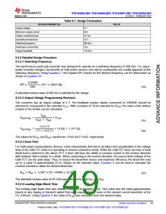
Table 9-1. Design Parameters
DESIGN PARAMETER
VALUE
Output voltage
5 V
Maximum output current
Output current pre-load
Operating temperature
Switching frequency
Peak input current limit
Target bandwidth
20 A
0.5 mA
25°C
500 kHz
14 A
~10 kHz
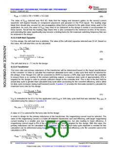
9.2.2 Detailed Design Procedure
9.2.2.1 Switching Frequency
The synchronous push-pull converter was designed to operate at a switching frequency of 500 kHz. For space-
grade converter designs, the benefits of GaN power devices over silicon counterparts are readily apparent at this
switching frequency. Using Equation 7, the required RT resistor for the desired frequency can be determined as
shown in Equation 24.
112000
RT =
19.7 = 204.3 kΩ
500
(24)
A standard resistor value of 205 kΩ is selected for the design.
9.2.2.2 Output Voltage Programming Resistors
The converter has an output voltage of 5 V. The feedback resistor divider connected to VSENSE should be
selected to correspond to the selected VOUT. With a resistor of 10 kΩ selected for RTOP, the value of the bottom
resistor in the divider can be calculated.
VREF
RBOTTOM
=
× RTOP
VOUT
VREF
(25)
(26)
0.613 V
5 V 0.613 V
RBOTTOM
=
× 10 k = 1.397 k
The values for RTOP and RBOT needed are 10 kΩ and 1.4 kΩ, respectively.
9.2.2.3 Dead Time
For GaN power semiconductor devices, a key characteristic that has to be taken into consideration is the voltage
drop of the GaN FET while it is operating in reverse conduction mode. While the GaN FET does not have a body
diode that is inherent in the silicon FET, it does still have the ability to conduct current in the reverse direction
with behavior that is similar to a diode. When conducting in the reverse direction, the source-drain voltage of the
GaN FET can be quite large. Thus, to reduce the dead-time losses and maximize efficiency, the dead time was
set to a value of approximately 25 ns. Based on the selected value, Equation 8 can be used to calculate the
resistors needed to attain the desired dead time.
RPS = RSP = 1.207 × 25 8.858 = 21.3 kΩ
(27)
The standard resistor value of 20.5 kΩ was selected for both RPS and RSP
.
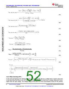
9.2.2.4 Leading Edge Blank Time
The leading edge blank time was initially chosen to be roughly 50 ns. This value was the initial approximation
based on any ringing or transient spikes that were expected to be seen on the sensed current waveform at the
CS_ILIM pin. Using Equation 9, the value of RLEB was calculated from this desired value.
Copyright © 2022 Texas Instruments Incorporated
Submit Document Feedback
49
Product Folder Links: TPS7H5005-SEP TPS7H5006-SEP TPS7H5007-SEP TPS7H5008-SEP

 TI [ TEXAS INSTRUMENTS ]