TPS7H5005-SEP, TPS7H5006-SEP, TPS7H5007-SEP, TPS7H5008-SEP
SLVSGG1 – FEBRUARY 2022
www.ti.com
RLEB = 1.212 × 50 9.484 = 51.1 kΩ
(28)
The value of RLEB selected was 49.9 kΩ. Note that the ringing and transient spikes on the sensed current
waveform will depend heavily on component placement and parastics in the PCB layout. The leading edge
blank time should also account for any propagation delay that is inherent to the gate driver being used in the
application. As such, the value of RLEB may need to be optimized as the design is tested in accommodate for
these factors. Recall that the leading edge blank time is also correlated to the minimum on-time of the device,
and extending this value significantly may become a limiting factor for the maximum switching frequency that can
be achieved in the design.
9.2.2.5 Soft-Start Capacitor
For this design, the soft-start time is arbitrary. The value of the soft-start capacitor selected was 33 nF. Based on
this value, the soft-start time can be calculated.
CSS × VREF
tSS
=
ISS
(29)
(30)
33 nF × 0.613 V
2.7 A
tSS
=
= 7.49 ms
The soft-start time is ~7.5 ms for the design.
9.2.2.6 Transformer
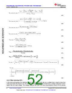
The turns ratio and primary inductance of the transformer will be determined based on the target specifications
of the converter. In order to calculate the maximum allowable turns ratio, a duty cycle limit must be selected for
the design. Even though DCL will be connected to AVSS to impose a 50% duty cycle limit from the controller
to ensure there is no overlap of the primary switching outputs, a maximum duty cycle of approximately 35% is
targeted for the design in order to provide sufficient margin to the controller limit. This is due to the fact that the
actual duty cycle is greater than calculated duty cycle when accounting for the converter efficiency, and to allow
for duty cycle increases during load transient events. Equation 31 provides the formulate needed to calculate the
maximum turns ratio for this design.
2 × V
× DLIM
IN_MIN
NPS_MAX
=
VOUT + VSR
(31)
VSR is estimated to be 0.5 V for the application and DLIM is 35% duty cycle limit that was selected. NPS_MAX is
calculated using the values in Equation 32.
2 × 22 V × 0.35
NPS_MAX
=
= 2.8
5 V + 0.5 V
(32)
A value of 2.5 is selected for the turns ratio for the design.
In order to design for the primary inductance of the transformer, the magnetizing current must be selected. The
value of the magnetizing current is a trade-off between transformer size and efficiency, with larger magnetizing
current leading to a smaller size due to lower required inductance, but also leading to lower efficiency. A
magnetizing current equal to 6% of the output current was initially targeted for this design. With this value, the
primary inductance can be calculated using Equation 36. The minimum duty cycle expected is needed for this
calculation can be determined using Equation 34, where the estimated efficiency η for the converter used in the
calculation is 85%.
VOUT + VSR
DMIN
=
2 × V
× NSP × η
IN_MAX
(33)
Copyright © 2022 Texas Instruments Incorporated
50
Submit Document Feedback
Product Folder Links: TPS7H5005-SEP TPS7H5006-SEP TPS7H5007-SEP TPS7H5008-SEP

 TI [ TEXAS INSTRUMENTS ]