TPS65142
www.ti.com
SLVSAX5 –JULY 2011
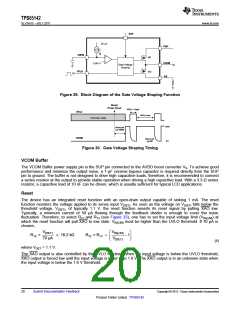
VDET
VDET_threshold+
Hys
VDET_threshold
Min. Operating
Voltage
1.6V
GND
Unknown state
XAO
GND
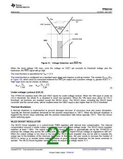
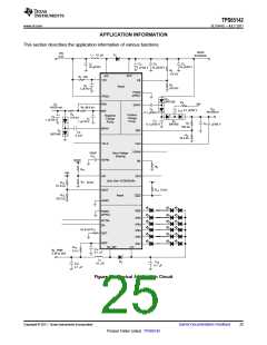
Figure 31. Voltage Detection and XAO Pin
When the input voltage VIN rises, once the voltage on VDET pin exceeds its threshold voltage plus the
hysteresis, the XAO signal will go high.
The reset function is operational for VIN ≥ 1.6 V.
The reset function is configured as a standard open-drain and requires a pull-up resistor. The resistor R(XAO) (R14
in Figure 33), which must be connected between the XAO pin output and a positive voltage VX greater than 2 V –
'high' logic level can be chosen as follows:
VX
VX - 2 V
R14
>
and
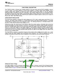
R14<
1 mA
2 μA
(5)
Under-voltage Lockout (UVLO)
The TPS65142 monitors both VIN and VBAT inputs for under-voltage lockout. When the VIN input in under its
UVLO threshold, the whole IC is disabled to avoid mis-operation. When the VIN input rises above its UVLO
threshold, all functions are enabled except the WLED driver. The WLED driver, including the WLED boost
converter and the current sinks, will be enabled when the VBAT input is also higher than its UVLO threshold.
Thermal Shutdown
A thermal shutdown is implemented to prevent damages because of excessive heat and power dissipation.
Typically the thermal shutdown threshold for the junction temperature is 150°C. When the thermal shutdown is
triggered the device stops switching until the junction temperature falls below typically 136°C. Then the device
starts switching again.
WLED BOOST REGULATOR
The WLED boost regulator is a current-mode PWM regulator with internal loop compensation. The internal
compensation ensures a stable output over the full input and output voltage range. The WLED boost regulator
switches at fixed 1 MHz. The output voltage of the boost regulator is automatically set by the TPS65142 to
minimize the voltage drop across the current-sink IFBx pins. The lowest IFB-pin voltage to regulated to 400 mV.
When the output voltage is too close to the input, the WLED boost regulator may not be able to regulate the
output due to the limitation of the minimum duty cycle. In that case, the user needs to increase the number of
WLED in series or to include series ballast resistors to provide enough headroom for the boost converter to
operate. The WLED boost regulator cannot regulate its output to a voltage below 15 V.
Copyright © 2011, Texas Instruments Incorporated
Submit Documentation Feedback
21
Product Folder Link(s) :TPS65142

 TI [ TEXAS INSTRUMENTS ]