TPS65142
SLVSAX5 –JULY 2011
www.ti.com
æ
ç
è
ö
VFB
VS
R3
=
» 18.2 kΩ
R2 = R3
´
-1
÷
70 μA
where VFBP = 1.240 V
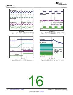
Soft-Start (AVDD Boost Converter)
VFB
ø
(1)
The AVDD boost converter has an internal digital soft-start to prevent high inrush current during start-up. The
typical soft-start time is 2ms.
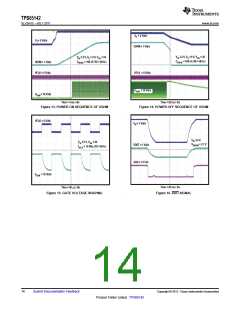
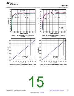
Frequency Select Pin (FREQ)
The digital frequency-select pin FREQ allows to set the switching frequency of the device to 650 kHz (FREQ =
low) or 1.2MHz (FREQ = high). Higher switching frequency improves load transient response but reduces slightly
the efficiency. The other benefit of a higher switching frequency is the lower output voltage ripple. Usually, it is
recommended to use1.2 MHz switching frequency unless light load efficiency is a major concern.
Overvoltage Protection
The AVDD boost converter has an integrated over-voltage protection to prevent the power switch from exceeding
the absolute maximum switch voltage rating at pin SW in case the feedback (FB) pin is floating or shorted to
GND. In such an event, the output voltage rises and is monitored with the overvoltage protection comparator
over the SUP pin. As soon as the comparator trips at typically 18 V, the boost converter turns the N-Channel
MOSFET switch off. The output voltage falls below the overvoltage threshold and the converter continues to
operate. In order to detect overvoltage, the SUP pin must to be connected to the output voltage of the boost
converter VS.
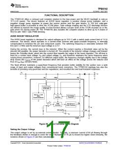
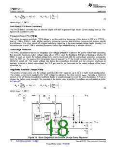
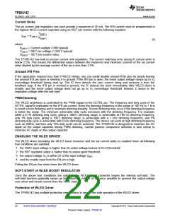
Regulated Positive Charge Pump
The positive charge pump sets the voltage applied on the VGH input pin, up to 32 V in tripler mode configuration.
The charge pump block regulates the VGH voltage by adjusting the drive current IDRVP. Typically, a minimum
current of 50 µA flowing through the feedback divider is usually enough to cover the noise fluctuation. If 70 µA is
chosen for higher noise immunity, the resistors of the divider used to set the VGH voltage are calculated as (refer
to Figure 26):
æ
ç
è
ö
VFBP
VGH
R8
=
» 18.2 kΩ
R7 = R8
´
-1
÷
70 μA
VFBP
ø
(2)
where VFBP = 1.240 V
VIN
VS
SW
SUP
SW
Clock of
Boost
Converter
?2
Positive
Charge
Pump
DRVP
Driver
VGH
R
7
FBP
R
8
VFBP
Figure 26. Block Diagram of the Positive Charge Pump Regulator
18
Submit Documentation Feedback
Copyright © 2011, Texas Instruments Incorporated
Product Folder Link(s) :TPS65142

 TI [ TEXAS INSTRUMENTS ]