TPS65142
www.ti.com
SLVSAX5 –JULY 2011
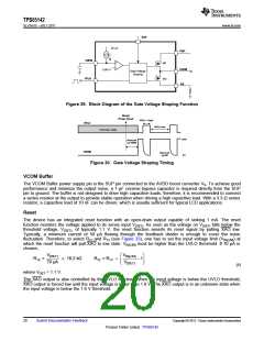
Current Limit Protection
The WLED boost regulator switching MOSFET has a pulse-by-pulse over-current limit of 1.5 A (minimum value).
The PWM switch turns off when the inductor current reaches this current threshold and remains off until the
beginning of the next switching cycle. This protects the IC and external components under over-load conditions.
When there is sustained overcurrent condition for more than 16 ms (under 100% dimming duty cycle), the IC
turns off and requires VBAT POR or the EN pin toggling to restart.
Under severe over load and/or short-circuit conditions, the VO pin can be pulled below the input (VBAT pin
voltage). Under this condition, the current can flow directly from the input to the output through the inductor and
the Schottky diode. Turning off the PWM switch alone does not limit current anymore. In this case, the
TPS65142 relies on the fuse at the input to protect the whole system. When the TPS65142 detects the output
voltage to be 1 V (short-circuit detection threshold) below the input voltage, it shuts down the WLED driver. The
IC restarts after input power-on reset (VBAT POR) or EN pin logic toggling.
Open WLED String Protection
If one of the WLED strings is open, the boost output rises to its over-voltage threshold (39V typically). The IC
detects the open WLED string by sensing no current in the corresponding IFBx pin. As a result, the IC removes
the open IFBx pin from the voltage feedback loop. The output voltage drops and is regulated to the voltage for
the remaining connected WLED strings. The IFBx current of the connected WLED string remains in regulation
during the whole transition.
The IC shuts down if it detects that all of the WLED strings are open.
Overvoltage Protection
If the overvoltage threshold is reached, but the current sensed on the IFBx pin is below the regulation target, the
IC regulates the boost output at the overvoltage threshold. This operation could occur when the WLED is turned
on under cold temperature, and the forward voltages of the WLEDs exceed the over-voltage threshold.
Maintaining the WLED current allows the WLED to warm up and their forward voltages to drop below the
overvoltage threshold.
If any IFBx pin voltage exceeds IFB overvoltage threshold (17 V typical), the IC turns off the corresponding
current sink and removes this IFB pin from VO regulation loop. The remaining IFBx pins’ current regulation is not
affected. This condition often occurs when there are several shorted WLEDs in one string. WLED mismatch
typically does not create such large voltage difference among WLED strings.
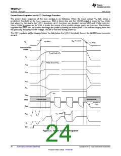
POWER UP/DOWN SEQUENCE
The power up and power down sequences are shown in Figure 32.
The operation of the bias converters are gated by the UVLO of the VIN voltage. The start-up of the WLED boost
converter is gated by the UVLO of the VBAT input, the power good of the REF output, the (VBAT-2 V) and VO
comparator output, and the EN input. The REF output is powered by the output of the AVDD boost converter
through the SUP pin; and hence, the WLED boost converter will not start before the AVDD boost converter.
Power Up Sequence
The power up sequence of the bias portion is as following. When the VIN rises above the ULVO threshold, and
the internal device enable signal is asserted. The AVDD boost converter begins the soft-start, the REF regulator
starts to rise, the VCOM buffer is enabled, and both charge pumps begins to operate. When the REF output
reaches its regulation voltage, a VREF power good signal is asserted for the WLED section. The AVDD boost
converter continues the soft start until its output voltage reaches the AVDD power good threshold when an AVDD
power good signal is asserted. The AVDD power good signal enables the 20µA current to the VDPM pin to start
the gate voltage shaping delay timer. The delay is programmed by the external capacitor connected to the VDPM
pin and should be long enough to ensure that both charge pumps are ready before the delay ends. Once the
delay ends, the gate voltage shaping (VGHM) output is enabled to be controlled by the VFLK input.
The power up sequence of the WLED driver section is as following. When the four conditions for the Enabling the
WLED Driver section are satisfied, the WLED boost converter begins the soft start, together with the start of the
current sinks. When any of the four conditions is not satisfied, the WLED boost converter will stop switching.
Copyright © 2011, Texas Instruments Incorporated
Submit Documentation Feedback
23
Product Folder Link(s) :TPS65142

 TI [ TEXAS INSTRUMENTS ]