TPS65142
SLVSAX5 –JULY 2011
www.ti.com
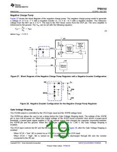
SUP
20 mA
VGH
VDPM
M1
M2
VGHM
1.240 V
Gate Voltage
Shaping
VFLK
RE
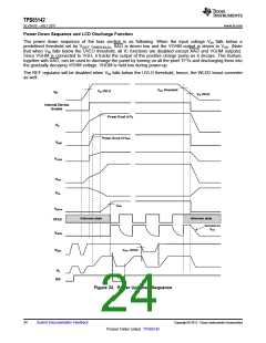
Figure 29. Block Diagram of the Gate Voltage Shaping Function
Boost
Power Good
VFKL = ’high’
VFLK
VFKL=’low’
Unknown state
VGH
Delay set
by VDPM
VGHM
Slope set
by RE
0V
Figure 30. Gate Voltage Shaping Timing
VCOM Buffer
The VCOM Buffer power supply pin is the SUP pin connected to the AVDD boost converter VS. To achieve good
performance and minimize the output noise, a 1-µF ceramic bypass capacitor is required directly from the SUP
pin to ground. The buffer is not designed to drive high capacitive loads; therefore, it is recommended to connect
a series resistor at the output to provide stable operation when driving a high capacitive load. With a 3.3-Ω series
resistor, a capacitive load of 10 nF can be driven, which is usually sufficient for typical LCD applications.
Reset
The device has an integrated reset function with an open-drain output capable of sinking 1 mA. The reset
function monitors the voltage applied to its sense input V(DET). As soon as the voltage on V(DET) falls below the
threshold voltage, V(DET), of typically 1.1 V, the reset function asserts its reset signal by pulling XAO low.
Typically, a minimum current of 50 µA flowing through the feedback divider is enough to cover the noise
fluctuation. Therefore, to select R12 and R13 (see Figure 33), one has to set the input voltage limit (VIN(LIM)) at
which the reset function will pull XAO to low state. VIN(LIM) must be higher than the UVLO threshold. If 70 µA is
chosen,
æ
ö
V
V
IN(LIM)
(DET)
R13
=
» 18.2 kΩ
R12 = R13
´
-1
ç
ç
è
÷
÷
ø
70 μA
V
(DET)
(4)
where VDET = 1.1 V.
The XAO output is also controlled by the UVLO function. When the input voltage is below the UVLO threshold,
XAO output is forced low until the input voltage is lower than 1.6 V. The XAO output is in an unknown state when
the input voltage is below the 1.6 V threshold.
20
Submit Documentation Feedback
Copyright © 2011, Texas Instruments Incorporated
Product Folder Link(s) :TPS65142

 TI [ TEXAS INSTRUMENTS ]