TPS65142
www.ti.com
SLVSAX5 –JULY 2011
FUNCTIONAL DESCRIPTION
The TPS65142 offers a compact and complete solution to the bias power and the WLED backlight in note-pc
TFT-LCD panels. The device features an AVDD boost regulator, a positive charge pump regulator, and a
negative charge pump regulator to power the source drivers and the gate drivers. A 150 mA unity-gain
high-speed buffer is provided to drive the VCOM plane. Gate voltage shaping and the LCD discharge function
are offered to improve the image quality. A reset function allows a proper reset of the TCON at power on or the
gate driver ICs during power off. The TPS65142 also includes the complete solution to drive up to 6 chains of
WLEDs with 1000:1 ratio PWM dimming.
AVDD BOOST REGULATOR
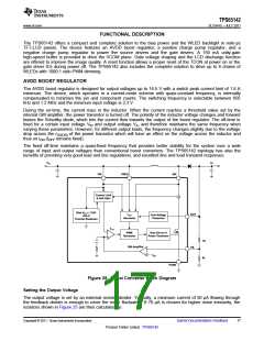
The AVDD boost regulator is designed for output voltages up to 16.5 V with a switch peak current limit of 1.8 A
minimum. The device, which operates in a current-mode scheme with quasi-constant frequency, is internally
compensated to minimize the pin and component counts. The switching frequency is selectable between 650
kHz and 1.2 MHz and the minimum input voltage is 2.3 V.
During the on-time, the current rises in the inductor. When the current reaches a threshold value set by the
internal GM amplifier, the power transistor is turned off. The polarity of the inductor voltage changes and forward
biases the Schottky diode, which lets the current flow towards the output of the boost regulator. The off-time is
fixed for a certain input voltage VIN and output voltage VS, and therefore maintains the same frequency when
varying these parameters. However, for different output loads, the frequency changes slightly due to the voltage
drop across the rDS(ON) of the power transistor which will have an effect on the voltage across the inductor and
thus on tON (tOFF remains fixed).
The fixed off-time maintains a quasi-fixed frequency that provides better stability for the system over a wide
range of input and output voltages than conventional boost converters. The TPS65142 topology has also the
benefits of providing very good load and line regulations, and excellent line and load transient responses.
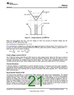
VS
VIN
VIN
FREQ
SW
Current Limit
& Soft Start
Bias VBG = 1.24V
UVLO
Thermal Shutdown
SUP
TOFF
Generator
Over-Voltage
Protection
TON
PWM
Generator
Gate Driver of
Power Transister
R
2
GM Amplifier
FB
VFB
R
3
PGND
Figure 25. Boost Converter Block Diagram
Setting the Output Voltage
The output voltage is set by an external resistor divider. Typically, a minimum current of 50 µA flowing through
the feedback divider is enough to cover the noise fluctuation. If 70 µA is chosen for higher noise immunity, the
resistors shown in Figure 25 are then calculated as:
Copyright © 2011, Texas Instruments Incorporated
Submit Documentation Feedback
17
Product Folder Link(s) :TPS65142

 TI [ TEXAS INSTRUMENTS ]