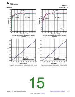
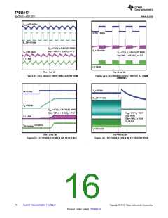
TPS65142
www.ti.com
SLVSAX5 –JULY 2011
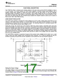
Negative Charge Pump
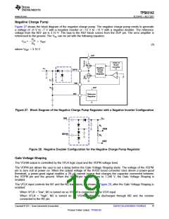
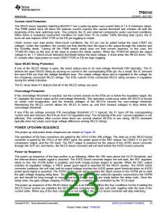
Figure 27 shows the block diagram of the negative charge pump. The negative charge pump needs to generate
a voltage of –6 V to –7 V with a negative inverter or –12 V to –13 V with a negative doubler. The reference
voltage from the REF pin is 3.15 V. The bias to the REF block comes from the SUP pin. The error amplifier is
referenced to the ground. The VGL can be set with the following equation:
R4
VGL = -
´ VREF
R5
(3)
where VREF = 3.15 V
SUP
Clock of
Boost
converter
?2
Negative
Charge
Pump
VGL
DRVN
Regulator
R4
R5
FBN
REF
SUP
Reference
Regulator
Figure 27. Block Diagram of the Negative Charge Pump Regulator with a Negative Inverter Configuration
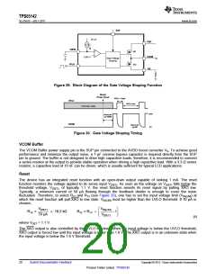
SW
VGL
R4
FBN
REF
DRVN
R5
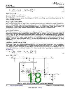
Figure 28. Negative Doubler Configuration for the Negative Charge Pump Regulator
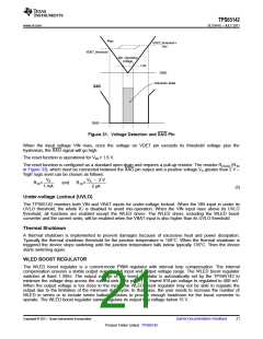
Gate Voltage Shaping
The VGHM output is controlled by the VFLK logic input and the VDPM voltage level.
The VDPM pin allows the user to set a delay before the Gate Voltage Shaping starts. The voltage of the VDPM
pin is zero volt at power on. When the output voltage of the AVDD boost converter rises above a power-good
threshold, a power-good signal enables a 20 µA current source that charges the capacitor connected between
the VDPM pin and the ground. When the VDPM-pin voltage rises to 1.240 V, the Gate Voltage Shaping is
enabled.
The VFLK input controls the M1 and the M2 transistors, as shown in Figure 29, after the Gate Voltage Shaping is
enabled:
When VFLK = “low”, M1 is turned on so VGHM is connected to the VGH input.
When VFLK = “high”, M2 is turned on so VGHM voltage is discharged through M2 and the resistor
connected to the RE pin.
Copyright © 2011, Texas Instruments Incorporated
Submit Documentation Feedback
19
Product Folder Link(s) :TPS65142

 TI [ TEXAS INSTRUMENTS ]