TPS55340
www.ti.com
SLVSBD4 –MAY 2012
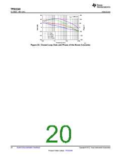
DESIGN GUIDE-STEP-BY-STEP DESIGN PROCEDURE OF SEPIC CONVERTER
Lb
La
TP4
VIN
VIN
6-18V
12V, 1A
1
TP5
49.9
TP2
VIN
86.6k
SYNC
SYNC
TP3
1
Not Populated
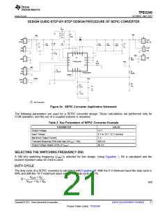
Figure 24. SEPIC Converter Application Schematic
The following parameters are used for a SEPIC converter design. These calculations are performed only for
CCM operation, and the use of a coupled inductor is assumed.
Table 2. Key Parameters of SEPIC Converter Example
PARAMETER
VALUE
Output Voltage
12 V
Input Voltage
6 V to 18 V, 12 V nominal
Maximum Output Current
1 A
Transient Response 50% load step (ΔVOUT = 4%)
Output Voltage Ripple (0.5% of VOUT
480 mV
60 mV
)
SELECTING THE SWITCHING FREQUENCY (R4)
A 500 kHz switching frequency (ƒSW) is selected for this design. Using Equation 1, R4 is calculated and the
nearest standard value 95.3 kΩ is used.
DUTY CYCLE
The duty cycle of a SEPIC converter is calculated with Equation 40. With the 6 V minimum input the duty cycle is
68% and with the 18 V maximum input voltage the duty cycle is 41%.
VOUT + VD
D =
VOUT + VD + V
IN
(40)
Copyright © 2012, Texas Instruments Incorporated
Submit Documentation Feedback
21
Product Folder Link(s) :TPS55340

 TI [ TEXAS INSTRUMENTS ]