TPS55340
SLVSBD4 –MAY 2012
www.ti.com
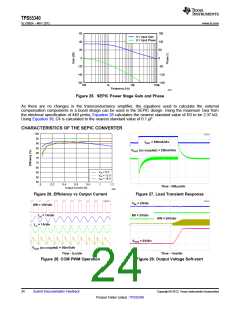
60
40
180
120
60
6 V Input Gain
6 V Input Phase
20
0
0
−20
−40
−60
−60
−120
−180
100
1k
10k
100k
Frequency (Hz)
G025
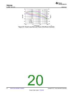
Figure 25. SEPIC Power Stage Gain and Phase
As there are no changes in the transconductance amplifier, the equations used to calculate the external
compensation components in a boost design can be used in the SEPIC design. Using the maximum Gea from
the electrical specification of 440 µmho, Equation 38 calculates the nearest standard value of R3 to be 2.37 kΩ.
Using Equation 39, C4 is calculated to the nearest standard value of 0.1 µF.
CHARACTERISTICS OF THE SEPIC CONVERTER
100
95
IOUT = 500mA/div
90
85
VOUT (ac coupled) = 200mV/div
80
75
70
65
VIN = 6 V
VIN = 12 V
VIN = 18 V
60
55
50
0
0.2
0.4
0.6
0.8
1
1.2
Time - 500ms/div
Output Current (A)
G026
Figure 26. Efficiency vs Output Current
Figure 27. Load Transient Response
VIN = 2V/div
SW = 10V/div
EN = 2V/div
ILb = 1A/div
ILa = 1A/div
SW = 20V/div
VOUT = 5V/div
VOUT (ac coupled) = 50mV/div
Time - 2ms/div
Time - 1ms/div
Figure 28. CCM PWM Operation
Figure 29. Output Voltage Soft-start
24
Submit Documentation Feedback
Copyright © 2012, Texas Instruments Incorporated
Product Folder Link(s) :TPS55340

 TI [ TEXAS INSTRUMENTS ]