TPS55340
www.ti.com
SLVSBD4 –MAY 2012
DIL
4´ ¦SW ´ CIN
DIL
Vripple =
I
(49)
(50)
ICIrms =
12
SELECTING THE SCHOTTKY DIODE (D1)
The selected diode must have a minimum breakdown voltage (VBR) calculated with Equation 51 which is 30.5 V
in this design. The average current rating is recommended to be greater than the maximum output current. With
the maximum 18 V input, average current is calculated to be 2.6 A using Equation 17. The package must also be
capable of handling the power dissipation. With an estimated 0.5V forward voltage, power dissipation is
calculated with Equation 26 to be 500mW. Diodes Inc B340B is chosen with a 40 V, 3 A rating in a SMB
package.
VBR = VO + VINmax + VF
(51)
SETTING THE OUTPUT VOLTAGE (R1, R2)
With R2 fixed at 10 kΩ using Equation 25 the nearest standard value of 86.6 kΩ is chosen for R1.
SETTING THE SOFT-START TIME (C3)
The recommended 0.047µF soft-start capacitor is used.
MOSFET RATING CONSIDERATIONS
In a SEPIC converter the MOSFET must be rated to handle the sum of the input and output voltages. In this
design with the maximum input voltage of 18 V and output voltage of 12 V the FET will see approximately 30 V.
A 10% tolerance is recommended to account for any ringing. The 40V rating of the TPS55340 power MOSFET
comfortably satisfies this requirement.
COMPENSATING THE CONTROL LOOP (R3, C4)
This design was compensated by measuring the frequency response of the power stage at the lowest input
voltage of 6 V and choosing the components for the desired bandwidth. The lowest right half plane zero (ƒRHPZ
)
is calculated to be 36.7kHz with Equation 52. Using the recommendation to limit the bandwidth to 1/3 of ƒRHPZ
the maximum recommended is 12.2kHz.
VOUT
IOUT
¦
=
RHPZ
æ
ö2
D
2´ p´L ´
ç
ç
÷
÷
1- D
(
)
è
ø
(52)
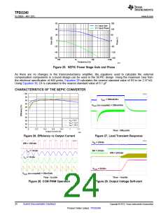
This design also uses only one pole and one zero. In order to achieve approximately 60 degrees of phase
margin, the power stage phase must be no lower than approximately –120 degrees at the desired bandwidth. To
ensure a stable design, R3 was initially set to 1kΩ and C4 was 1µF. Figure 25 shows the measurement of the
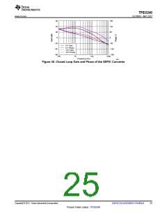
power stage At 7kHz the power stage has a gain of 19.52 dB and phase of –118.1 degrees.
Copyright © 2012, Texas Instruments Incorporated
Submit Documentation Feedback
23
Product Folder Link(s) :TPS55340

 TI [ TEXAS INSTRUMENTS ]