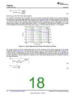
TPS55340
SLVSBD4 –MAY 2012
www.ti.com
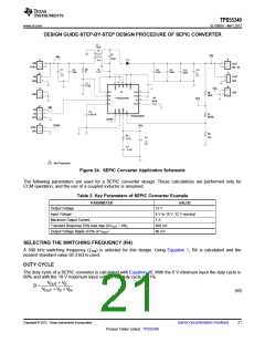
SELECTING THE INDUCTOR (L1)
With an estimated 85% efficiency, the input current is calculated with Equation 9 to be 2.35 A. With KIND of 0.3
and the maximum 18 V input the minimum inductance is calculated to be 10.5µH using Equation 41. The nearest
standard value of 12µH is used. As mentioned previously, this equation assumes a coupled inductor is used.
V max´Dmin
IN
L ³
2´ ¦SW ´I DC´KIND
IN
(41)
The inductor ripple current is recalculated to be 615mA with Equation 42. The peak current is calculated to
3.69 A. The typical current limit is used as the saturation rating for the inductor used. The RMS current for La is
approximately the average input current 2.35 A. The RMS current for Lb is approximately the output current of
1 A. For this design a CoilCraft MSD1260-123 is used with 6.86 A saturation, 74 mΩ DCR and 3.12 A RMS
current rating for one winding.
V max´Dmin
IN
DIL =
2´ ¦SW ´L
(42)
DIL
DIL
æ
ö
æ
ö
ILpeak = ILapeak +ILbpeak = I DC +
+ I
èç OUT
+
÷
÷
èç IN
ø
ø
2
2
(43)
CALCULATING THE MAXIMUM OUTPUT CURRENT
The maximum output current with the minimum input voltage 6 V, chosen inductance 12µH, 5.25 A minimum
current limit and estimated 85% efficiency is calculated to be 1.47 A using Equation 44.
I
LIM - DIL
I
LIM -I DC´KIND
(
)
(
)
IN
IOUT max =
=
æ
ç
è
ö
÷
ø
æ
ç
è
ö
VOUT
VOUT
+1
+1
÷
ø
V min´ hEST
V min´ hEST
IN
IN
(44)
SELECTING THE OUTPUT CAPACITOR (C8-C10)
To meet the 60 mV ripple specification, the minimum output capacitance is calculated to be 22.5µF with
Equation 45. This design uses ceramic output capacitors and the effects of ESR are ignored. To meet the
transient response of 500mA with less than 480mV voltage change and a 7kHz control loop bandwidth, the
minimum output capacitance is calculated to be 23.7µF using Equation 46. The RMS current is calculated with
Equation 22 to be 1.44 A. The output capacitors used in this design is 3 x 22 µF, 25 V X7R 1210 ceramic
capacitors. With voltage derating, the effective total output capacitance is estimated to be 30.4 µF.
Dmax ´ IOUT
COUT
³
¦
´ VRIPPLE
SW
(45)
(46)
DITRAN
2p´ ¦BW ´ DVTRAN
COUT
³
SELECTING THE SERIES CAPACITOR (C6)
The series capacitor is chosen to limit the ripple current to 5% of the maximum input voltage. Using Equation 47
the minimum capacitance is 1.5 µF. Using Equation 48 the RMS current is calculated to be 1.63A. A 2.2 µF
ceramic capacitor in a 1206 package is selected.
IOUT ´ Dmax
CP ³
0.05 ´ V max ´ ƒSW
IN
(47)
(48)
(1- Dmax)
ICPrms = I DC ´
IN
Dmax
SELECTING THE INPUT CAPACITOR (C2, C7)
Based on the minimum 4.7µF ceramic recommended for the TPS55340, a 10µF X7R input capacitor is used with
an additional 0.1µF placed close to the VIN and GND pins. With an estimated 6 µF capacitance after voltage
derating, the input ripple voltage is calculated to be 39.9mV using Equation 49. The RMS current of the input
capacitance is calculated to be 0.177 A with Equation 50.
22
Submit Documentation Feedback
Copyright © 2012, Texas Instruments Incorporated
Product Folder Link(s) :TPS55340

 TI [ TEXAS INSTRUMENTS ]