TPS5430
www.ti.com
SLVS632–JANUARY 2006
APPLICATION INFORMATION (continued)
0.110
0.220
0.080
0.013 DIA 4 PL
0.040
0.098
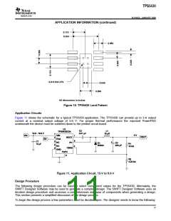
All dimensions in inches
Figure 10. TPS5430 Land Pattern
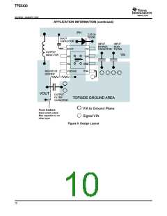
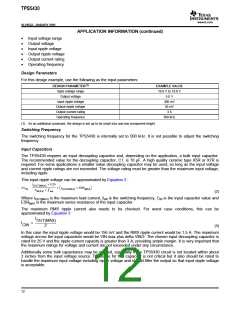
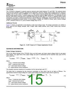
Application Circuits
Figure 11 shows the schematic for a typical TPS5430 application. The TPS5430 can provide up to 3-A output
current at a nominal output voltage of 5.0 V. For proper thermal performance the exposed PowerPAD
underneath the device must be soldered down to the printed circuit board.
U1
C2
0.01 mF
L1
15 mH
TPS5430DDA
VIN
10.8 - 19.8 V
7
5 V
VIN
1
8
4
VOUT
BOOT
5
EN
ENA
NC
2
3
6
C1
10 mF
+
PH
C3
220 mF
D1
B340A
R1
NC
10 kW
VSNS
GND
PwPd
9
R2
3.24 kW
Figure 11. Application Circuit, 12-V to 5.0-V
Design Procedure
The following design procedure can be used to select component values for the TPS5430. Alternately, the
SWIFT Designer Software may be used to generate a complete design. The SWIFT Designer Software uses an
iterative design procedure and accesses a comprehensive database of components when generating a design.
This section presents a simplified discussion of the design process.
To begin the design process a few parameters must be decided upon. The designer needs to know the following:
11

 TI [ TEXAS INSTRUMENTS ]