TPS5430
www.ti.com
SLVS632–JANUARY 2006
APPLICATION INFORMATION (continued)
Thermal Shutdown
The TPS5430 protects itself from overheating with an internal thermal shutdown circuit. If the junction
temperature exceeds the thermal shutdown trip point, the voltage reference is grounded and the high-side
MOSFET is turned off. The part is restarted under control of the slow start circuit automatically when the junction
temperature drops 14°C below the thermal shutdown trip point.
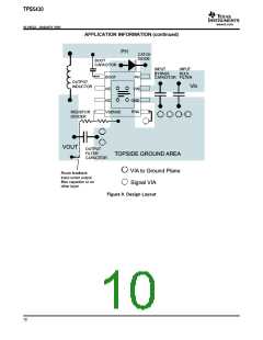
PCB Layout
Connect a low ESR ceramic bypass capacitor to the VIN pin. Care should be taken to minimize the loop area
formed by the bypass capacitor connections, the VIN pin, and the TPS5430 ground pin. The best way to do this
is to extend the top side ground area from under the device adjacent to the VIN trace, and place the bypass
capacitor as close as possible to the VIN pin. The minimum recommended bypass capacitance is 10 uF ceramic
with a X5R or X7R dielectric.
There should be a ground area on the top layer directly underneath the IC, with an exposed area for connection
to the PowerPAD. Use vias to connect this ground area to any internal ground planes. Use additional vias at the
ground side of the input and output filter capacitors as well. The GND pin should be tied to the PCB ground by
connecting it to the ground area under the device as shown below.
The PH pin should be routed to the output inductor, catch diode and boot capacitor. Since the PH connection is
the switching node, the inductor should be located very close to the PH pin and the area of the PCB conductor
minimized to prevent excessive capacitive coupling. The catch diode should also be placed close to the device to
minimize the output current loop area. Connect the boot capacitor between the phase node and the BOOT pin as
shown. Keep the boot capacitor close to the IC and minimize the conductor trace lengths. The component
placements and connections shown work well, but other connection routings may also be effective.
Connect the output filter capacitor(s) as shown between the VOUT trace and GND. It is important to keep the
loop formed by the PH pin, Lout, Cout and GND as small as is practical.
Connect the VOUT trace to the VSENSE pin using the resistor divider network to set the output voltage. Do not
route this trace too close to the PH trace. Due to the size of the IC package and the device pin-out, the trace
may need to be routed under the output capacitor. Alternately, the routing may be done on an alternate layer if a
trace under the output capacitor is not desired.
If the grounding scheme shown is utilized, use a via connection to a different layer to route to the ENA pin.
9

 TI [ TEXAS INSTRUMENTS ]