TPS5430
www.ti.com
SLVS632–JANUARY 2006
Catch Diode
The TPS5430 is designed to operate using an external catch diode between PH and GND. The selected diode
must meet the absolute maximum ratings for the application: Reverse voltage must be higher than the maximum
voltage at the PH pin, which is VINMAX + 0.5 V. Peak current must be greater than IOUTMAX plus on half the
peak to peak inductor current. Forward voltage drop should be small for higher efficiencies. It is important to note
that the catch diode conduction time is typically longer than the high-side FET on time, so attention paid to diode
parameters can make a marked improvement in overall efficiency. Additionally, check that the device chosen is
capable of dissipating the power losses. For this design, a Diodes, Inc. B340A is chosen, with a reverse voltage
of 40 V, forward current of 3 A, and a forward voltage drop of 0.5V.
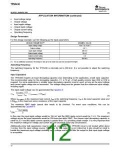
Additional Circuits
Figure 12 shows an application circuit utilizing a wide input voltage range. The design parameters are simillar to
those given for the design example, with a larger value output inductor and a lower closed loop crosover
frequency.
U1
L1
C2
TPS5430DDA
5 V
22 mH
12–35 V
0.01 mF
7
5
2
VIN
1
VIN
ENA
NC
VOUT
BOOT
EN
C1
10 mF
8
+
PH
C3
220 mF
3
D1
R1
4
NC
6
10 kW
VSNS
GND
SBL845
PwPd
9
R2
3.24 kW
Figure 12. 12-35 V Input to 5 V Output Application Circuit
ADVANCED INFORMATION
Output Voltage Limitations
Due to the internal design of the TPS5430, there are both upper and lower output voltage limits for any given
input voltage. The upper limit of the output voltage set point is constrained by the maximum duty cycle of 87%
and is given by:
V
ǒ
0.87
V
I
0.230 ) V
I
R
V
OUTMAX
INMIN
OMAX
D
OMAX
L
D
(13)
Where
VINMIN = minimum input voltage
IOMAX = maximum load current
VD = catch diode forward voltage.
RL= output inductor series resistance.
This equation assumes maximum on resistance for the internal high side FET.
The lower limit is constrained by the minimum controllable on time which may be as high as 200nsec. The
approximate minimum output voltage for a given input voltage and minimum load current is given by:
V
ǒ
0.12
V
I
0.110 ) V
I
R
V
OUTMIN
INMAX
OMIN
D
OMIN
L
D
(14)
Where
VINMAX = maximum input voltage
IOMIN = minimum load current
VD = catch diode forward voltage.
RL= output inductor series resistance.
15

 TI [ TEXAS INSTRUMENTS ]