TPS5430
www.ti.com
SLVS632–JANUARY 2006
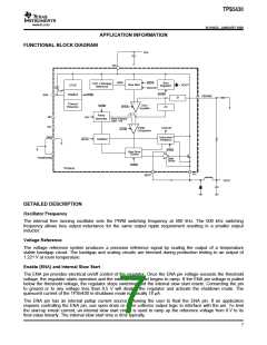
APPLICATION INFORMATION (continued)
Undervoltage Lockout (UVLO)
The TPS5430 incorporates an under voltage lockout circuit to keep the device disabled when VIN (the input
voltage) is below the UVLO start voltage threshold. During power up, internal circuits are held inactive until VIN
exceeds the UVLO start threshold voltage. Once the UVLO start threshold voltage is reached, device start-up
begins. The device operates until VIN falls below the UVLO stop threshold voltage. The typical hysteresis in the
UVLO comparator is 330 mV.
Boost Capacitor (BOOT)
Connect a 0.01 µF low-ESR ceramic capacitor between the BOOT pin and PH pin. This capacitor provides the
gate drive voltage for the high-side MOSFET. X7R or X5R grade dielectrics are recommended due to their stable
values over temperature.
Output Feedback (VSENSE) and Internal Compensation
The output voltage of the regulator is set by feeding back the center point voltage of an external resistor divider
network to the VSENSE pin. In steady-state operation, the VSENSE pin voltage should be equal to the voltage
reference 1.221 V.
The TPS5430 implements internal compensation to simplify the regulator design. Since the TPS5430 uses
voltage mode control, a type 3 compensation network has been designed on chip to provide a high crossover
frequency and a high phase margin for good stability. Refer to Internal Compensation Network in the applications
section for more details.
Voltage Feed Forward
The internal voltage feed forward provides a constant DC power stage gain despite any variations with the input
voltage. This greatly simplifies the stability analysis and improves the transient response. Voltage feed forward
varies the peak ramp voltage inversely with the input voltage so that the modulator and power stage gain are
constant at the feed forward gain, i.e.
VIN
Feed Forward Gain )
Ramp
pk pk
(1)
The typical feed forward gain of TPS5430 is 25.
Pulse-Width-Modulation (PWM) Control
The regulator employs a fixed frequency pulse-width-modulator (PWM) control method. First, the feedback
voltage (VSENSE pin voltage) is compared to the constant voltage reference by the high gain error amplifier and
compensation network to produce a error voltage. Then, the error voltage is compared to the ramp voltage by the
PWM comparator. In this way, the error voltage magnitude is converted to a pulse width which is the duty cycle.
Finally, the PWM output is fed into the gate drive circuit to control the on-time of the high-side MOSFET.
Overcurrent Protection
Overcurrent protection is implemented by sensing the drain-to-source voltage across the high-side MOSFET.
The drain to source voltage is then compared to a voltage level representing the overcurrent threshold limit. If the
drain-to-source voltage exceeds the overcurrent threshold limit, the overcurrent indicator is set true. The system
will ignore the overcurrent indicator for the leading edge blanking time at the beginning of each cycle to avoid any
turn-on noise glitches.
Once overcurrent indicator is set true, overcurrent protection is triggered. The high-side MOSFET is turned off for
the rest of the cycle after a propagation delay. The overcurrent protection scheme is called cycle-by-cycle current
limiting.
If the sensed current continues to increase during cycle-by-cycle current limiting, the hiccup mode overcurrent
protection will be triggered instead of cycle-by-cycle current limiting. During hiccup mode overcurrent protection,
the voltage reference is grounded and the high-side MOSFET is turned off for the hiccup time. Once the hiccup
time duration is complete, the regulator restarts under control of the slow start circuit.
8

 TI [ TEXAS INSTRUMENTS ]