TPS5430
www.ti.com
SLVS632–JANUARY 2006
APPLICATION INFORMATION
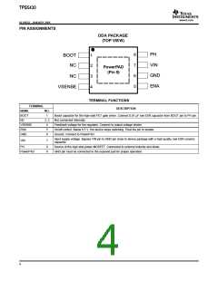
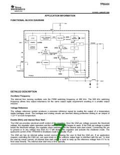
FUNCTIONAL BLOCK DIAGRAM
VIN
VIN
VREF
SHDN
Boot
Regulator
1.221 V Bandgap
Slow Start
UVLO
BOOT
Reference
HICCUP
5 µA
SHDN
ENABLE
ENA
SHDN
VSENSE
Z1
Thermal
Error
SHDN
SHDN
Z2
Protection
Amplifier
Ramp
NC
VIN
Feed Forward
Generator
Gain = 25
NC
HICCUP
PWM
SHDN
Comparator
GND
Overcurrent
Oscillator
SHDN
Protection
SHDN
Gate Drive
Control
POWERPAD
Gate
Driver
SHDN
TPS5430
PH
BOOT
VOUT
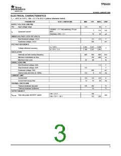
DETAILED DESCRIPTION
Oscillator Frequency
The internal free running oscillator sets the PWM switching frequency at 500 kHz. The 500 kHz switching
frequency allows less output inductance for the same output ripple requirement resulting in a smaller output
inductor.
Voltage Reference
The voltage reference system produces a precision reference signal by scaling the output of a temperature
stable bandgap circuit. The bandgap and scaling circuits are trimmed during production testing to an output of
1.221 V at room temperature.
Enable (ENA) and Internal Slow Start
The ENA pin provides electrical on/off control of the regulator. Once the ENA pin voltage exceeds the threshold
voltage, the regulator starts operation and the internal slow start begins to ramp. If the ENA pin voltage is pulled
below the threshold voltage, the regulator stops switching and the internal slow start resets. Connecting the pin
to ground or to any voltage less than 0.5 V will disable the regulator and activate the shutdown mode. The
quiescent current of the TPS5430 in shutdown mode is typically 18 µA.
The ENA pin has an internal pullup current source, allowing the user to float the ENA pin. If an application
requires controlling the ENA pin, use open drain or open collector output logic to interface with the pin. To limit
the start-up inrush current, an internal slow start circuit is used to ramp up the reference voltage from 0 V to its
final value linearly. The internal slow start time is 8ms typically.
7

 TI [ TEXAS INSTRUMENTS ]