TPS5430-Q1
www.ti.com ................................................................................................................................................... SLVS751C–NOVEMBER 2007–REVISED JULY 2009
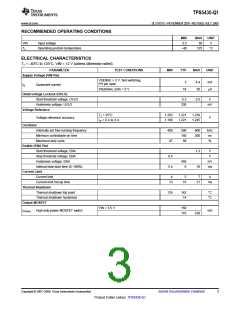
RECOMMENDED OPERATING CONDITIONS
MIN
5.5
MAX
36
UNIT
V
VIN
TJ
Input voltage
Operating junction temperature
–40
125
°C
ELECTRICAL CHARACTERISTICS
TJ = –40°C to 125°C, VIN = 12 V (unless otherwise noted)
PARAMETER
TEST CONDITIONS
MIN
TYP
MAX
UNIT
Supply Voltage (VIN Pin)
VSENSE = 2 V, Not switching,
PH pin open
3
4.4
50
mA
IQ
Quiescent current
Shutdown, ENA = 0 V
18
µA
Undervoltage Lockout (UVLO)
Start threshold voltage, UVLO
Hysteresis voltage, UVLO
Voltage Reference
5.3
5.5
V
330
mV
TJ = 25°C
1.202
1.196
1.221
1.221
1.239
1.245
Voltage reference accuracy
Oscillator
V
IO = 0 A to 3 A
Internally set free-running frequency
Minimum controllable on time
Maximum duty cycle
400
87
500
150
89
600
200
kHz
ns
%
Enable (ENA Pin)
Start threshold voltage, ENA
Stop threshold voltage, ENA
Hysteresis voltage, ENA
1.3
10
V
V
0.5
5.4
450
8
mV
ms
Internal slow-start time (0~100%)
Current Limit
Current limit
4
5
7
A
Current-limit hiccup time
13
16
21
ms
Thermal Shutdown
Thermal shutdown trip point
Thermal shutdown hysteresis
135
162
14
°C
°C
Output MOSFET
VIN = 5.5 V
150
110
rDS(on) High-side power MOSFET switch
mΩ
230
Copyright © 2007–2009, Texas Instruments Incorporated
Submit Documentation Feedback
3
Product Folder Link(s): TPS5430-Q1

 TI [ TEXAS INSTRUMENTS ]