TPS5430-Q1
SLVS751C–NOVEMBER 2007–REVISED JULY 2009................................................................................................................................................... www.ti.com
These devices have limited built-in ESD protection. The leads should be shorted together or the device placed in conductive foam
during storage or handling to prevent electrostatic damage to the MOS gates.
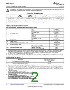
ORDERING INFORMATION(1)
INPUT
VOLTAGE
OUTPUT
VOLTAGE
TJ
PACKAGE(2)
PART NUMBER
–40°C to 125°C
5.5 V to 36 V
Adjustable to 1.22 V
Thermally-enhanced SOIC (DDA)
TPS5430QDDARQ1
(1) For the most current package and ordering information, see the Package Option Addendum at the end of this document, or see the TI
web site at www.ti.com.
(2) Package drawings, thermal data, and symbolization are available at www.ti.com/packaging.
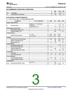
ABSOLUTE MAXIMUM RATINGS(1) (2)
over operating free-air temperature range (unless otherwise noted)
VIN
–0.3 V to 40 V(3)
–0.3 V to 50 V
–0.6 V to 40 V(3)
–0.3 V to 7 V
10 V
BOOT
PH (steady state)
VI
Input voltage range
ENA
BOOT-PH
VSENSE
–0.3 V to 3 V
–1.2 V
PH (transient < 10 ns)
IO
Source current
PH
PH
Internally Limited
10 µA
Ilkg
TJ
Leakage current
Operating virtual-junction temperature range
Storage temperature range
–40°C to 150°C
–65°C to 150°C
1500 V
Tstg
Human-body model (HBM)
Machine model (MM)
ESD
Electrostatic discharge rating
200 V
Charged-device model (CDM)
1500 V
(1) Stresses beyond those listed under absolute maximum ratings may cause permanent damage to the device. These are stress ratings
only and functional operation of the device at these or any other conditions beyond those indicated under recommended operating
conditions is not implied. Exposure to absolute-maximum-rated conditions for extended periods may affect device reliability.
(2) All voltage values are with respect to network ground terminal.
(3) Approaching the absolute maximum rating for the VIN pin may cause the voltage on the PH pin to exceed the absolute maximum rating.
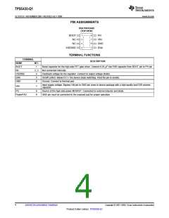
DISSIPATION RATINGS(1) (2)
THERMAL IMPEDANCE
JUNCTION-TO-AMBIENT
PACKAGE
8-pin DDA (2-layer board with solder)(3)
8-pin DDA (4-layer board with solder)(4)
33°C/W
26°C/W
(1) Maximum power dissipation may be limited by overcurrent protection.
(2) Power rating at a specific ambient temperature TA should be determined with a junction temperature of 125°C. This is the point where
distortion starts to substantially increase. Thermal management of the final PCB should strive to keep the junction temperature at or
below 125°C for best performance and long-term reliability. See Thermal Calculations in applications section of this data sheet for more
information.
(3) Test board conditions:
a. 3 in × 3 in, two layers, thickness: 0.062 in
b. 2-oz copper traces located on the top and bottom of the PCB
c. Six thermal vias in the thermal pad area under the device package
(4) Test board conditions:
a. 3 in × 3 in, four layers, thickness: 0.062 in
b. 2-oz copper traces located on the top and bottom of the PCB
c. 2-oz copper ground planes on the two internal layers
d. Six thermal vias in the thermal pad area under the device package
2
Submit Documentation Feedback
Copyright © 2007–2009, Texas Instruments Incorporated
Product Folder Link(s): TPS5430-Q1

 TI [ TEXAS INSTRUMENTS ]