TPS51216
SLUSAB9 –NOVEMBER 2010
www.ti.com
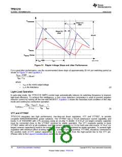
V
VDDQSNS
Slope (1)
Jitter
(2)
(1)
Slope (2)
Jitter
20 mV
V
REFIN
V
+Noise
REFIN
t
t
OFF
UDG-10139
ON
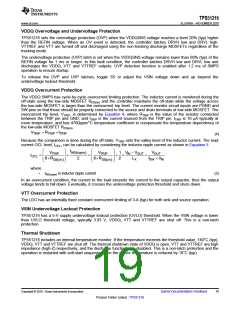
Figure 31. Ripple Voltage Slope and Jitter Performance
For a good jitter performance, use the recommended down slope of approximately 20 mV per switching period as
shown in Figure 31 and Equation 2.
V
´ESR
OUT
³ 20mV
f
´L
SW
X
where
•
•
VOUT is the VDDQ output voltage
LX is the inductance
(2)
Light-Load Operation
In auto-skip mode, the TPS51216 SMPS control logic automatically reduces its switching frequency to improve
light-load efficiency. To achieve this intelligence, a zero cross detection comparator is used to prevent negative
inductor current by turning off the low-side MOSFET. Equation 3 shows the boundary load condition of this skip
mode and continuous conduction operation.
V
- V
OUT ) V
´
(
1
IN
OUT
I
=
´
LOAD(LL)
2´L
V
f
SW
X
IN
(3)
VTT and VTTREF
TPS51216 integrates two high performance, low-drop-out linear regulators, VTT and VTTREF, to provide
complete DDR2/DDR3/DDR3L power solutions. The VTTREF has a 10-mA sink/source current capability, and
tracks ½ of VDDQSNS with ±1% accuracy using an on-chip ½ divider. A 0.22-mF (or larger) ceramic capacitor
must be connected close to the VTTREF terminal for stable operation. The VTT responds quickly to track
VTTREF within ±40 mV at all conditions, and the current capability is 2 A for both sink and source. A 10-mF (or
larger) ceramic capacitor(s) need to be connected close to the VTT terminal for stable operation. To achieve tight
regulation with minimum effect of wiring resistance, a remote sensing terminal, VTTSNS, should be connected to
the positive node of VTT output capacitor(s) as a separate trace from the high-current line to the VTT pin.
(Please refer to the Layout Considerations section for details.)
18
Submit Documentation Feedback
Copyright © 2010, Texas Instruments Incorporated
Product Folder Link(s) :TPS51216

 TI [ TEXAS INSTRUMENTS ]