TPS51216
SLUSAB9 –NOVEMBER 2010
www.ti.com
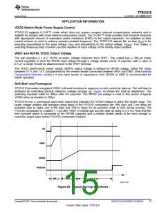
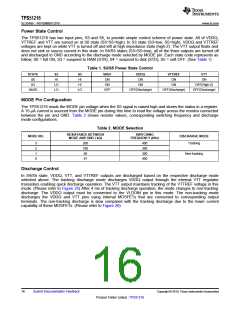
Power State Control
The TPS51216 has two input pins, S3 and S5, to provide simple control scheme of power state. All of VDDQ,
VTTREF and VTT are turned on at S0 state (S3=S5=high). In S3 state (S3=low, S5=high), VDDQ and VTTREF
voltages are kept on while VTT is turned off and left at high impedance state (high-Z). The VTT output floats and
does not sink or source current in this state. In S4/S5 states (S3=S5=low), all of the three outputs are turned off
and discharged to GND according to the discharge mode selected by MODE pin. Each state code represents as
follow; S0 = full ON, S3 = suspend to RAM (STR), S4 = suspend to disk (STD), S5 = soft OFF. (See Table 1)
Table 1. S3/S5 Power State Control
STATE
S0
S3
HI
S5
HI
VREF
ON
VDDQ
ON
VTTREF
ON
VTT
ON
S3
LO
LO
HI
ON
ON
ON
OFF(High-Z)
OFF(Discharge)
S4/S5
LO
OFF
OFF(Discharge)
OFF(Discharge)
MODE Pin Configuration
The TPS51216 reads the MODE pin voltage when the S5 signal is raised high and stores the status in a register.
A 15-mA current is sourced from the MODE pin during this time to read the voltage across the resistor connected
between the pin and GND. Table 2 shows resistor values, corresponding switching frequency and discharge
mode configurations.
Table 2. MODE Selection
RESISTANCE BETWEEN
MODE AND GND ( kΩ)
SWITCHING
FREQUENCY (kHz)
MODE NO.
DISCHARGE MODE
3
2
1
0
200
100
68
400
300
300
400
Tracking
Non-tracking
47
Discharge Control
In S4/S5 state, VDDQ, VTT, and VTTREF outputs are discharged based on the respective discharge mode
selected above. The tracking discharge mode discharges VDDQ output through the internal VTT regulator
transistors enabling quick discharge operation. The VTT output maintains tracking of the VTTREF voltage in this
mode. (Please refer to Figure 25) After 4 ms of tracking discharge operation, the mode changes to non-tracking
discharge. The VDDQ output must be connected to the VLDOIN pin in this mode. The non-tracking mode
discharges the VDDQ and VTT pins using internal MOSFETs that are connected to corresponding output
terminals. The non-tracking discharge is slow compared with the tracking discharge due to the lower current
capability of these MOSFETs. (Please refer to Figure 26)
16
Submit Documentation Feedback
Copyright © 2010, Texas Instruments Incorporated
Product Folder Link(s) :TPS51216

 TI [ TEXAS INSTRUMENTS ]