TPS51216
www.ti.com
SLUSAB9 –NOVEMBER 2010
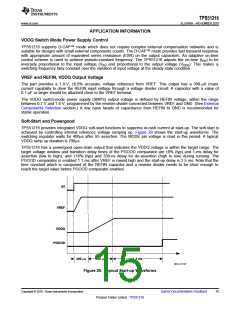
D-CAP™ Mode
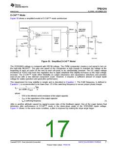
Figure 30 shows a simplified model of D-CAP™ mode architecture.
V
IN
VDDQSNS
9
High-Side
MOSFET
DRVH
14
PWM
+
Lx
REFIN
VDDQ
Control
Logic
and
8
6
ESR
R
LOAD
VREF
Driver
R1
Low-Side
MOSFET
DRVL
+
C
11
OUT
1.8 V
R2
UDG-10136
Figure 30. Simplified D-CAP™ Model
The VDDQSNS voltage is compared with REFIN voltage. The PWM comparator creates a set signal to turn on
the high-side MOSFET. The gain and speed of the comparator is high enough to maintain the voltage at the
beginning of each on-cycle (or the end of each off-cycle) to be substantially constant. The DC output voltage
monitored at VDDQ may have line regulation due to ripple amplitude that slightly increases as the input voltage
increase. The D-CAP™ mode offers flexibility on output inductance and capacitance selections and provides
ease-of-use with a low external component count. However, it requires a sufficient amount of output ripple
voltage for stable operation and good jitter performance.
The requirement for loop stability is simple and is described in Equation 1. The 0-dB frequency, f0 defined in
Equation 1, is recommended to be lower than 1/3 of the switching frequency to secure proper phase margin.
f
1
SW
f =
£
0
2p´ESR ´C
3
OUT
where
•
•
•
ESR is the effective series resistance of the output capacitor
COUT is the capacitance of the output capacitor
fsw is switching frequency
(1)
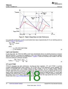
Jitter is another attribute caused by signal-to-noise ratio of the feedback signal. One of the major factors that
determine jitter performance in D-CAP™ mode is the down-slope angle of the VDDQSNS ripple voltage.
Figure 31 shows, in the same noise condition, a jitter is improved by making the slope angle larger.
Copyright © 2010, Texas Instruments Incorporated
Submit Documentation Feedback
17
Product Folder Link(s) :TPS51216

 TI [ TEXAS INSTRUMENTS ]