TPS51216
SLUSAB9 –NOVEMBER 2010
www.ti.com
Layout Considerations
Certain issues must be considered before designing a layout using the TPS51216.
2
TPS51216
VLDOIN
VIN
VTT
VTT
3
10 mF
VTTGND
VTTGND
4
V5IN
#1
12
V
OUT
VTTREF
MODE
TRIP
1 mF
#2
5
DRVL
PGND
0.22 mF
11
10
19
18
#3
VREF
REFIN GND
8 7
6
0.1 mF
10 nF
UDG-10166
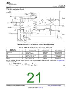
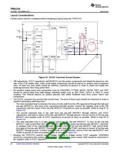
Figure 33. DC/DC Converter Ground System
•
•
•
VIN capacitor(s), VOUT capacitor(s) and MOSFETs are the power components and should be placed on one
side of the PCB (solder side). Other small signal components should be placed on another side (component
side). At least one inner plane should be inserted, connected to ground, in order to shield and isolate the
small signal traces from noisy power lines.
All sensitive analog traces and components such as VDDQSNS, VTTSNS, MODE, REFIN, VREF and TRIP
should be placed away from high-voltage switching nodes such as SW, DRVL, DRVH or VBST to avoid
coupling. Use internal layer(s) as ground plane(s) and shield feedback trace from power traces and
components.
The DC/DC converter has several high-current loops. The area of these loops should be minimized in order to
suppress generating switching noise.
–
–
–
The most important loop to minimize the area of is the path from the VIN capacitor(s) through the high and
low-side MOSFETs, and back to the capacitor(s) through ground. Connect the negative node of the VIN
capacitor(s) and the source of the low-side MOSFET at ground as close as possible. (Refer to loop #1 of
Figure 33)
The second important loop is the path from the low-side MOSFET through inductor and VOUT
capacitor(s), and back to source of the low-side MOSFET through ground. Connect source of the low-side
MOSFET and negative node of VOUT capacitor(s) at ground as close as possible. (Refer to loop #2 of
Figure 33)
The third important loop is of gate driving system for the low-side MOSFET. To turn on the low-side
MOSFET, high current flows from V5IN capacitor through gate driver and the low-side MOSFET, and back
to negative node of the capacitor through ground. To turn off the low-side MOSFET, high current flows
from gate of the low-side MOSFET through the gate driver and PGND, and back to source of the low-side
MOSFET through ground. Connect negative node of V5IN capacitor, source of the low-side MOSFET and
PGND at ground as close as possible. (Refer to loop #3 of Figure 33)
•
Because the TPS51216 controls output voltage referring to voltage across VOUT capacitor, VDDQSNS
should be connected to the positive node of VOUT capacitor. In a same manner GND should be connected to
the negative node of VOUT capacitor.
22
Submit Documentation Feedback
Copyright © 2010, Texas Instruments Incorporated
Product Folder Link(s) :TPS51216

 TI [ TEXAS INSTRUMENTS ]