TPS51640A, TPS59640, TPS59641
www.ti.com
SLUSAQ2 –JANUARY 2012
PCB LAYOUT GUIDELINE
SCHEMATIC REVIEW
Because the voltage and current feedback signals are fully differential it is a good idea to double check their
polarity.
1. CCSP1/CCSN1
2. CCSP2/CCSN2
3. CCSP2/CCSN2
4. GCSP/GCSN
5. VCCSENSE to CVFB/VSSSENSE to CGFB (for CPU)
6. VCCGTSENSE to GVFB/VSSGTSENSE to GGFB (for GPU)
Also, note the order of the current sense inputs on Pin 4 to Pin 9 as the second phase has a reverse order.
CAUTION
Separate noisy driver interface lines from sensitive analog interface lines: (This is the
MOST CRITICAL LAYOUT RULE)
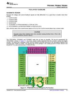
The TPS51640A, TPS59640, and TPS59641 make this as easy as possible. The pin-out arrangement for
TPS51640A is shown in Figure 71. The driver outputs clearly separated from the sensitive analog and digital
circuitry. The driver has a separate PGND and this should be directly connected to the decoupling capacitor that
connects from V5DRV to PGND. The thermal pad of the package is the analog ground for these devices and
should NOT be connected directly to PGND (Pin 42).
CTHERM 1
36 CPWM3
35 CSKIP
34 GPWM
33 GSKIP
32 GTHERM
31 GOCP-I
30 GIMON
29 GCSP
COCP-I
CIMON
CCSP1
CCSN1
CCSN2
CCSP2
CCSP3
CCSN3
2
3
4
5
6
7
8
9
GND
28 GCSN
27 GCOMP
26 GVFB
CCOMP 10
CVFB 11
CGFB 12
25 GGFB
Drivers
Analog
Digital
Power
Figure 71. TPS51640A Pin-out Arranged by Pin Function
Copyright © 2012, Texas Instruments Incorporated
Submit Documentation Feedback
43

 TI [ TEXAS INSTRUMENTS ]