TPS1HC100-Q1
ZHCSLK6A –JULY 2021 –REVISED DECEMBER 2021
www.ti.com.cn
10 Power Supply Recommendations
The device is qualified for both automotive and industrial applications. The normal power supply connection is a
12-V automotive system. The supply voltage must be within the range specified in the Recommended Operating
Conditions.
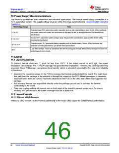
VBB Voltage Range
Note
Extended lower 12-V automotive battery operation such as cold crank and start-stop. Device is fully functional
but current sense and current limit accuracies do not apply as well as timing parametrics can deviate from
specification.
3 V to 6 V
Nominal 12-V automotive battery voltage range. All parametric specifications apply and the device is fully
functional and protected.
6 V to 18 V
18 V to 28 V
35 V
Extended upper 12-V automotive battery operation such as double battery. Device is fully functional and
protected but timing parametrics can deviate from specifications
Load dump voltage. Device is operational and lets the pulse pass through without being damaged but does not
protect against short circuits.
11 Layout
11.1 Layout Guidelines
To prevent thermal shutdown, TJ must be less than 150°C. If the output current is very high, the power
dissipation can be large. The HTSSOP package has good thermal impedance. However, the PCB layout is very
important. Good PCB design can optimize heat transfer, which is absolutely essential for the long-term reliability
of the device.
• Maximize the copper coverage on the PCB to increase the thermal conductivity of the board. The major heat-
flow path from the package to the ambient is through the copper on the PCB. Maximum copper is extremely
important when there are not any heat sinks attached to the PCB on the other side of the board opposite the
package.
• Add as many thermal vias as possible directly under the package ground pad to optimize the thermal
conductivity of the board.
• Plate shut or plug and cap all thermal vias on both sides of the board to prevent solder voids. To ensure
reliability and performance, the solder coverage must be at least 85%.
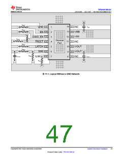
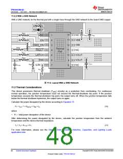
11.2 Layout Example
11.2.1 Without a GND Network
Without a GND network, tie the thermal pad directly to the board GND copper for better thermal performance.
Copyright © 2022 Texas Instruments Incorporated
46
Submit Document Feedback
Product Folder Links: TPS1HC100-Q1

 TI [ TEXAS INSTRUMENTS ]