TPS1H100-Q1
ZHCSDD8D –OCTOBER 2014–REVISED DECEMBER 2019
www.ti.com.cn
MAX UNIT
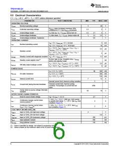
6.5 Electrical Characteristics
5 V < VS < 40 V; –40°C < TJ < 150°C unless otherwise specified
PARAMETER
OPERATING VOLTAGE
TEST CONDITIONS
MIN
TYP
VS,nom
Nominal operating voltage
5
40
5
V
V
RDS(on) value increases maximum 20%,
compared to 5 V, see RDS(on) parameter
VS,op
Extended operating voltage
3.5
VS,UVR
VS,UVF
VUV,hys
Undervoltage restart
VS rises up, VS > VS,UVR, device turn on
VS falls down, VS < VS,UVF, device shuts off
3.5
3
3.7
3.2
0.5
4
V
V
V
Undervoltage shutdown
3.5
Undervoltage shutdown, hysteresis
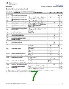
OPERATING CURRENT
VIN = 5 V, VDIAG_EN = 0 V, no load
5
mA
Inom Nominal operating current
VIN = 5 V, VDIAG_EN = 0 V, 10-Ω load
10 mA
VS = 13.5 V, VIN = VDIAG_EN = VCS = VCL
VOUTPUT = 0 V, TJ = 25°C
=
=
0.5
5
µA
µA
Ioff
Standby current
VS = 13.5 V, VIN = VDIAG_EN = VCS = VCL
VOUTPUT = 0 V, TJ = 125°C
Ioff,diag
toff,deg
Standby current with diagnostic enabled VIN = 0 V, VDIAG_EN = 5 V
1.2 mA
ms
IN from high to low, if deglitch time > toff,deg
,
Standby mode deglitch time(1)
2
enters into standby mode.
VS = 13.5 V, VIN = VOUTPUT = 0, TJ = 25°C
0.5
3
µA
µA
Ileak,out
Off-state output leakage current
VS = 13.5 V, VIN = VOUTPUT = 0, TJ = 125°C
POWER STAGE
VS > 5 V, TJ = 25°C
VS > 5 V, TJ = 150°C
VS = 3.5 V, TJ = 25°C
80
100 mΩ
166 mΩ
120 mΩ
RDS-ON
On-state resistance
Ilim,nom
Internal current limit
7
13
A
A
Internal current limit, thermal cycling condition
5
External current limit, thermal cycling
condition; Percentage of current limit set
value
Ilim,tsd
Current limit during thermal shutdown
50%
Clamp drain-to-source voltage internally
clamped
VDS
50
70
V
OUTPUT DIODE CHARACTERISTICS
VF
Drain-to-source diode voltage
VIN = 0, IOUT = −0.2 A
0.7
4
V
A
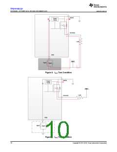
t < 60 s, VS = 13.5 V, GND pin 1-kΩ resistor
in parallel with diode. TJ = 25°C. See Irev1 test
condition (Figure 6).
Continuous reverse current when
reverse polarity(2)
Irev1
Continuous reverse current when
VOUT > VS + Vdiode
t < 60 s, VS = 13.5 V. TJ = 25°C. See Irev2
test condition (Figure 7).
Irev2
2
A
(2)
LOGIC INPUT (IN AND DIAG_EN)
Vlogic,h Input or DIAG_EN high-level voltage
Vlogic,l
Vlogic,hys
Rpd,in
2
V
V
Input or DIAG_EN low-level voltage
Input or DIAG_EN hysteresis voltage
Input pulldown resistor
0.8
250
500
150
mV
kΩ
kΩ
Rpd,diag
Diag pulldown resistor
(1) Value is specified by design, not subject to production test.
(2) Value is based on the minimum value of the 10 pcs/3 lots samples.
6
Copyright © 2014–2019, Texas Instruments Incorporated

 TI [ TEXAS INSTRUMENTS ]