TPS1H100-Q1
ZHCSDD8D –OCTOBER 2014–REVISED DECEMBER 2019
www.ti.com.cn
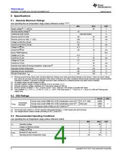
MAX UNIT
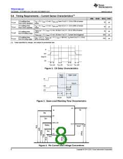
6.6 Timing Requirements – Current Sense Characteristics(1)
MIN NOM
CS settling time
from DIAG disabled value.
VIN = 5 V, Iload ≥ 5 mA. VDIAG_EN from 5 to 0 V. CS to 10% of sense
tCS,off1
tCS,on1
10
10
µs
µs
CS settling time
from DIAG enabled value.
VIN = 5 V, Iload ≥ 5 mA. VDIAG_EN from 0 to 5 V. CS to 90% of sense
VDIAG_EN = 5 V, Iload ≥ 5 mA. IN from 5 to 0 V. CS to 10% of sense
value.
10
180
150
µs
µs
µs
CS settling time
from IN falling edge
tCS,off2
VDIAG_EN = 5 V, Iload ≥ 5 mA. IN from 5 to 0 V. Current limit triggered.
CS settling time
from IN rising edge
VVS = 13.5 V, VDIAG_EN = 5 V, Iload ≥ 100 mA. VIN from 0 to 5 V. CS to
90% of sense value.
tCS,on2
(1) Value specified by design, not subject to production test.
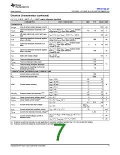
In
Iout
Diag-En
CS
Tcs, on2
Tcs, off1
Tcs, on1 Tcs, off2
Figure 2. CS Delay Characteristics
Open
Load
Open Load
Vcs,H
In
CS
ST
Tol,off
Tol,on
Tol,off
Figure 3. Open-Load Blanking Time Characteristics
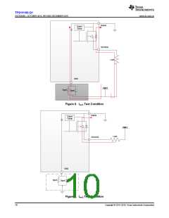
VS
IS
IN
IIN
ST
IST
DIAG_EN
OUT
IDIAG
IOUT
CL
ICL
GND
CS
ICS
Figure 4. Pin Current and Voltage Conventions
8
Copyright © 2014–2019, Texas Instruments Incorporated

 TI [ TEXAS INSTRUMENTS ]