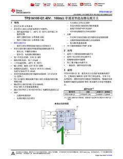
TPS1H100-Q1
www.ti.com.cn
ZHCSDD8D –OCTOBER 2014–REVISED DECEMBER 2019
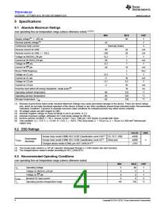
6.4 Thermal Information
TPS1H100-Q1
THERMAL METRIC(1)
PWP (HTSSOP)
UNIT
14 PINS
41
(2)
RθJA
Junction-to-ambient thermal resistance
Junction-to-case (top) thermal resistance
Junction-to-board thermal resistance
°C/W
°C/W
°C/W
°C/W
°C/W
°C/W
RθJC(top)
RθJB
29.7
25.1
0.9
ψJT
Junction-to-top characterization parameter
Junction-to-board characterization parameter
Junction-to-case (bottom) thermal resistance
ψJB
24.8
2.7
RθJC(bot)
(1) For more information about traditional and new thermal metrics, see the Semiconductor and IC Package Thermal Metrics application
report.
(2) The thermal data is based on JEDEC standard high-K profile – JESD 51-7. The copper pad is soldered to the thermal land pattern. Also,
correct attachment procedure must be incorporated.
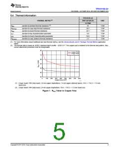
80
4-layer PCB
2-layer PCB
70
60
50
40
30
20
0
100
200
300
400
500
600
700
800
Copper Area (mm2)
D025
(1) 4-layer board: FR4 2s2p board, 2.8-mil copper (top/bottom), 1.4-mil copper (internal layers). 76.4- × 114.3- × 1.5-mm
board size.
(2) 2-layer board: FR4 2s0p board, 2.8-mil copper (top/bottom). 76.4- × 114.3- × 1.5-mm board size.
Figure 1. RθJA Value vs Copper Area
Copyright © 2014–2019, Texas Instruments Incorporated
5

 TI [ TEXAS INSTRUMENTS ]