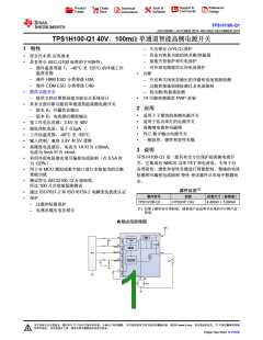
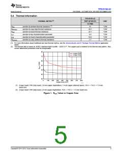
TPS1H100-Q1
www.ti.com.cn
ZHCSDD8D –OCTOBER 2014–REVISED DECEMBER 2019
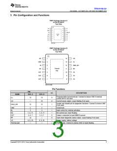
5 Pin Configuration and Functions
PWP Package Version A
14-Pin HTSSOP
Top View
NC
GND
IN
1
2
3
4
5
6
7
14
13
12
11
10
9
ST
CL
DIAG_EN
NC
Thermal
Pad
NC
OUT
OUT
OUT
VS
VS
8
VS
Not to scale
PWP Package Version B
14-Pin HTSSOP
Top View
NC
GND
IN
1
2
3
4
5
6
7
14
13
12
CS
CL
DIAG_EN
NC
Thermal
Pad
NC
11
10
9
OUT
OUT
OUT
VS
VS
8
VS
Not to scale
Pin Functions
PIN
I/O
DESCRIPTION
NAME
VER. A
VER. B
Programmable current-limit pin. Connect to device GND if external
current limit is not used.
CL
CS
13
—
12
13
14
12
O
O
I
Current-sense output. Leave floating if not used.
Enable and disable pin for diagnostic functions. Connect to device GND
if not used.
DIAG_EN
GND
2
3
2
3
—
I
Ground pin
IN
Input control for channel activation
NC
1, 4, 11
5, 6, 7
14
1, 4, 11
5, 6, 7
—
—
O
O
I
No-connect pin; leave floating.
OUT
Output, connected to load (NMOS source)
Open-drain diagnostic status output. Leave floating if not used.
Power supply; battery voltage
ST
VS
8, 9, 10
—
8, 9, 10
—
Thermal pad
—
Thermal pad. Connect to device GND or leave floating.
Copyright © 2014–2019, Texas Instruments Incorporated
3

 TI [ TEXAS INSTRUMENTS ]