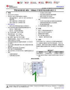
TPS1H100-Q1
ZHCSDD8D –OCTOBER 2014–REVISED DECEMBER 2019
www.ti.com.cn
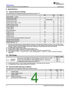
6 Specifications
6.1 Absolute Maximum Ratings
over operating free-air temperature range (unless otherwise noted)
(1)(2)(3)
MIN
MAX
UNIT
V
Supply voltage(4), t < 400 ms
Reverse polarity voltage(5)
Continuous drain current
Reverse current on GND
Reverse current on GND, t < 120 s
Voltage on IN/DIAG_EN pin
Current on IN /DIAG_EN pin
Voltage on ST pin
48
–18
V
Internally limited
A
–50
–250
–0.3
–30
20
20
7
mA
mA
V
2
mA
V
–0.3
–30
7
Current on ST pin
10
2
mA
KHz
V
IN pin PWM frequency
Voltage on CL pin
–0.3
–2
7
Current on CL pin
30
6.5
30
70
125
150
150
mA
V
Voltage on CS pin
–2.7
–2
Current on CS pin
mA
mJ
°C
°C
°C
Inductive load switch-off energy dissipation, single pulse(6)
Operating ambient temperature
Operating junction temperature
Storage temperature, Tstg
–40
–40
–65
(1) Stresses beyond those listed under Absolute Maximum Ratings may cause permanent damage to the device. These are stress ratings
only, which do not imply functional operation of the device at these or any other conditions beyond those indicated under Recommended
Operating Conditions. Exposure to absolute-maximum-rated conditions for extended periods may affect device reliability.
(2) All voltage values are with respect to GND.
(3) Absolute negative voltage on these terminals is not to go below –0.3 V.
(4) Absolute maximum voltage, withstand 48-V load dump voltage for 400 ms.
(5) Reverse polarity condition: t < 60 s, reverse current < Irev1, GND pin 1-kΩ resistor in parallel with diode.
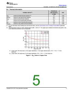
(6) Test condition: VS = 13.5 V, L = 8 mH, R = 0 Ω, TJ = 150°C. FR4 2s2p board, 2- × 70-μm Cu, 2- × 35-μm Cu. 600-mm2 thermal pad
copper area.
6.2 ESD Ratings
VALUE
±5000
±4000
±750
UNIT
Human body model (HBM) AEC-Q100 Classification Level H3A(1) VS, OUT, GND
Electrostatic
discharge
V(ESD)
Human body model (HBM) AEC-Q100 Classification Level H2(1)
Charged device model (CDM), per AEC Q100-011(2)
Other pins
V
(1) The human-body model is a 107-pF capacitor discharged through a 1.5-kΩ resistor into each terminal.
(2) The charged-device model is tested according to AEC_Q100-011C.
6.3 Recommended Operating Conditions
over operating free-air temperature range (unless otherwise noted)
MIN
5
MAX
40
5
UNIT
VS
Operating voltage
V
V
Voltage on IN/DIAG_EN pin
Voltage on ST pin
0
0
5
V
Io,nom
TJ
Nominal DC load current
Operating junction temperature range
0
4
A
–40
150
°C
4
Copyright © 2014–2019, Texas Instruments Incorporated

 TI [ TEXAS INSTRUMENTS ]