TMS3705
www.ti.com
11-07-22-003 – SCBS881B –JANUARY 2010–REVISED APRIL 2010
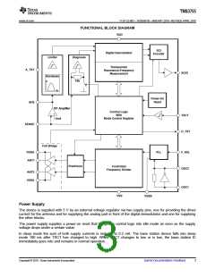
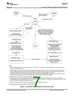
FUNCTIONAL BLOCK DIAGRAM
VDD
SCI
Encoder
Digital Demodulator
Limiter
Diagnosis
Transponder
Resonance-Frequency
Measurement
A_TST
SCIO
Bandpass
10k
Power-On
Reset
SFB
RF Amplifier
Control Logic
With
Mode Control Register
TXCT
Vref
SENSE
D_TST
Full Bridge
F_SEL
OSC2
PLL
VDDA
ANT1
Predrivers
Controlled
Frequency Divider
ANT2
VSSA
OSC1
VSS
VSSB
Power Supply
The device is supplied with 5 V by an external voltage regulator via two supply pins, one for providing the driver
current for the antenna and for supplying the analog part in front of the digital demodulator and one for supplying
the other blocks.
The power supply supplies a power-on reset that brings the control logic into idle mode as soon as the supply
voltage drops under a certain value.
In sleep mode the sum of both supply currents is reduced to 0.2 mA. The base station device falls into sleep
mode 100 ms after TXCT has changed to high. When TXCT changes to low or is low, the base station IC
immediately goes into and remains in normal operation.
Copyright © 2010, Texas Instruments Incorporated
Submit Documentation Feedback
3

 TI [ TEXAS INSTRUMENTS ]