TMS320TCI6487
TMS320TCI6488
Communications Infrastructure Digital Signal Processor
www.ti.com
SPRS358F–APRIL 2007–REVISED AUGUST 2008
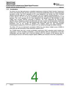
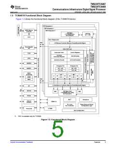
1.3 TCI6487/8 Functional Block Diagram
Figure 1-2 shows the functional block diagram of the TCI6487/8 device.
DSP Subsystem 2
DSP Subsystem 1
32
DDR2 Memory
DSP Subsystem 0
Controller
32K Bytes
L2/Cache
0.5 - 1.5 M
L1P SRAM/Cache
Direct-Mapped
PLL2
C64x+ Megamodule
L1P Memory Controller (Memory Protect/Bandwidth Mgmt)
2
Serial RapidIO
(2x)
C64x+ DSP Core
Instruction Fetch
Control Registers
SPLOOP Buffer
TCP2
VCP2
16-/32-bit
Instruction Dispatch
Instruction Decode
In-Circuit Emulation
McBSP0
McBSP1
A Register File
B Register File
A31 - A16
A15 - A0
B31 - B16
B15 - B0
EMAC
.M1
.M2
10/100/1000
.L1
.S1
xx
xx
.D1
.D2
xx
xx
.S2
.L2
SGMII
MDIO
L1 Data Memory Controller (Memory Protect/Bandwidth Mgmt)
I2C
16
GPIO16
FSYNC
32K Bytes Total
RSA
RSA
L1D SRAM/Cache 2-Way
Set Associative
RAC(A)
Semaphore
Antenna
Interface
EDMA 3.0
PLL1 and
Power-Down and Device
Configuration Logic
PLL1 Controller
L3 ROM
Timer [0-5]
Boot Configuration
A. RAC is available only for TCI6488.
Figure 1-2. Functional Block Diagram
Submit Documentation Feedback
Features
5

 TI [ TEXAS INSTRUMENTS ]