TMS320TCI6487
TMS320TCI6488
Communications Infrastructure Digital Signal Processor
SPRS358F–APRIL 2007–REVISED AUGUST 2008
www.ti.com
Contents
1
Features ................................................... 1
5.7 Megamodule Revision............................... 64
1.1
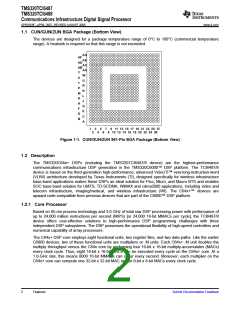
CUN/GUN/ZUN BGA Package (Bottom View) ....... 2
5.9
C64X+ Megamodule Register Description(s) ....... 64
1.2 Description............................................ 2
1.2.1 Core Processor ...................................... 2
1.2.2 Peripherals ........................................... 3
1.2.3 Accelerators.......................................... 4
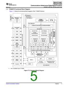
1.3 TCI6487/8 Functional Block Diagram ................ 5
6
7
Rake Search Accelerator (RSA) ..................... 72
Device Operating Conditions ........................ 73
7.1
Absolute Maximum Ratings Over Operating Case
Temperature Range (Unless Otherwise Noted)..... 73
7.2 Recommended Operating Conditions............... 74
7.3
Electrical Characteristics Over Recommended
Ranges of Supply Voltage and Operating Case
Temperature (Unless Otherwise Noted) ............ 75
Revision History............................................... 7
2
Device Overview ......................................... 8
2.1 Device Characteristics................................ 8
2.2 CPU (DSP Core) Description......................... 9
2.3 Memory Map Summary ............................. 12
2.4 Boot Sequence...................................... 15
2.5 Pin Assignments .................................... 18
2.6 Signal Groups Description .......................... 22
2.7 Terminal Functions.................................. 27
2.8 Development ........................................ 42
Device Configuration .................................. 46
3.1 Device Configuration at Device Reset .............. 46
8
Peripheral Information and Electrical
Specifications ........................................... 76
8.1 Parameter Information .............................. 76
8.2
Recommended Clock and Control Signal Transition
Behavior ............................................. 77
8.3 Power Supplies...................................... 77
8.4
Enhanced Direct Memory Access (EDMA3)
Controller ............................................ 79
8.5 Interrupts........................................... 102
8.6 Reset Controller.................................... 109
8.7 PLL1 and PLL1 Controller ......................... 114
8.8 PLL2 and PLL2 Controller ......................... 128
8.9 DDR2 Memory Controller .......................... 130
8.10 I2C Peripheral...................................... 133
8.11 Multichannel Buffered Serial Port (McBSP)........ 138
8.12 Ethernet MAC (EMAC)............................. 142
8.13 Management Data Input/Output (MDIO)........... 149
8.14 Timers.............................................. 151
8.15 Enhanced Viterbi-Decoder Coprocessor (VCP2) .. 160
8.16 Enhanced Turbo Decoder Coprocessor (TCP2)... 162
8.17 Serial RapidIO (SRIO) Port ........................ 164
8.18 General Purpose Input/Output (GPIO)............. 176
8.19 Emulation Features and Capability ................ 177
8.20 Semaphore......................................... 181
8.21 Antenna Interface Subsystem ..................... 184
8.22 Frame Synchronization ............................ 197
8.23 RAC (TCI6488 Only)............................... 201
Mechanical Data....................................... 202
9.1 Thermal Data ...................................... 202
9.2 Packaging Information ............................. 202
3
3.2
Peripheral Selection After Device Reset ............ 46
3.3 Device State Control Registers ..................... 47
3.4 Device Status Register Descriptions ................ 48
3.5
Inter-DSP Interrupt Registers (IPCGR0-IPCGR2
and IPCAR0-IPCAR2)............................... 50
3.6
JTAG ID (JTAGID) Register Description ............ 51
3.7 Debugging Considerations .......................... 51
4
5
System Interconnect................................... 52
4.1
Internal Buses, Switch Fabrics, and
Bridges/Gaskets..................................... 52
4.2 Data Switch Fabric Connections .................... 53
4.3 Configuration Switch Fabric ......................... 54
4.4 Priority Allocation.................................... 56
C64x+ Megamodule.................................... 57
5.1 Megamodule Diagram............................... 57
5.2 Memory Architecture ................................ 58
5.3 Memory Protection .................................. 61
5.4 Bandwidth Management ............................ 63
5.5 Power-Down Control ................................ 63
5.6 Megamodule Resets ................................ 64
9
6
Contents
Submit Documentation Feedback

 TI [ TEXAS INSTRUMENTS ]